
 Case Report
Effect of Infrared Radiation on the Hydrogen in Thin Films Double Barriers Based Melt Silicone-Germany
Received Date: December 08, 2018; Published Date: December 17, 2018
Abstract
Possibilities of plasma chemical deposition of α-Si1-x Gex:H (x=0÷1) films undoped and doped with PH3 or B2H6 have been analyzed from the viewpoint of their application in p-i-n structures of solar cell. The optical properties are considered, and the amount of hydrogen contained in those films is determined. The film properties are found to strongly depend on the film composition and the hydrogenation level. The number of hydrogen atoms in the films is varied by changing the gas mixture composition, and IR absorption in α-Si:H and α-Ge:H films is measured. The α-Si:H and а-Si0,88Ge1,2:H films were used to fabricate three-layer solar with an element area of 1,3 sm2 and an efficiency (η) of 9.5 %.
Keywords: Effect infrared on thin films; Amorphous silicon; Solar cells; Efficiency; Optical properties; Oscillator; Absorption coefficient; Effusion of hydrogen; Deposition rate
Introduction
Introduction of Si films and its alloy characterized by various structural phases. The most interesting of them are crystals that are in the amorphous matrix. Such alloys are produced by different methods at different technological regimes. For films of amorphous hydrogenated silicon and a-Si: H, formed by the method of cyclic sedimentation annealed in hydrogen plasma effect Staeblera- Vronsky is expressed weakly [1]. Authors [2] note the absence of the effect of Stajeblera-Vronsky in Nanostructure films of a-Si:H film Silicon alloys crystallization of a-Si: H is carried out by various methods: long annealing in vacuum at 600 °C, fast heat treatment [3], laser annealing [4] and ion implantation [5]. The mobility of the charge carriers, alloying and efficiency optical absorption coefficient in films of a-Si: H vy she than crystalline silicon. Films a-Si1-xGex: H are an effective and inexpensive material for making solar cells and other electronic devices [6, 7].
In this regard, the receipt of the aforementioned films and changing their conductivity type are actual tasks. [8] shows that with the change in the temperature of the substrate grow Nano crystals increases. Found that with increasing concentration of average grain size decreases RN3 (d) and the proportion of crystalline particle volume (Vc). When alloying with increasing concentration of boron, B2H6, value (d) does not change, and Vc is reduced. The value of photo films and efficiency-Si1-xGex: H, somewhat lower than in a-Si: H [9, 10]. With the changing conditions of technology and technological parameters of hydrogen deposited on various structural phases: microcrystalline, polycrystalline, Nana crystalline, etc. of energy conversion efficiency based on Schottky barrier in films of a-Si: H was 5.5%. Attempts have been made to obtain high efficiency solar cell (CPA ASE) (~ 9.0%) on the basis of a-Si1-xGex: H [11]. Most literature data show that when using amorphous silicon and Silicon-Germanium alloys in solar cells with multilayered or cascading structure have the greatest EFFICIENCY ~ 8.5% [12]. Based on the above stated the purpose of this work is to determine the amount of hydrogen in amorphous films method for optical solid solution a-Si1-xGex: H (x = 0-1) and manufacturing of solar cells based on them.
The Experimental Part
Thin films of a-Si1-xGex: H (x = 0-1) received plasma chemical deposition method using gas mixtures of H2 + SiH4, U + GeH4 in various proportions. Details on obtaining films shown in [11, 12]. Plasma RF field created through mainly inductive coupling. Film thickness was 0.1 ÷ 1.0 μm. Measured absorption coefficient (α), refraction (n), reflection (R), (T), width of band gap (E0) for each sample, using appropriate models [13.14]. Optical absorption at room temperature were studied by the method of [13-16] on spectrometer x-29.
Result and Discussion
The hydrogen concentration in a-Si1-xGe1-x: H, (x = 0 ÷ 1) films is determined using the method of Brodsky et al. [14 - 17]:

where N is the number of Avogadro and (ξ) the integral strength of the hydride with units cm2/mole (g/ξ) = 3.5. If the width of the absorption indicate through and center frequency ω*, ω0, when Δ ω/ω0 ≤ 0.1 after approximation with a tolerance of ± 2%, equation (1) can be written as follows:

where is: 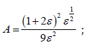 ε- dielectric constant. For Si, ε=12; Ge, ε =16.
If the equation (2) preintegral expression Relabel АSи
 – the cumulative uptake of fashion streching for each film, then in determining hydrogen concentration (NH) get a general expression in abbreviated form:

Coefficient АS– for films a-Si:H, is in the field of fashion stretching 1,4∙1020 см-2. Absorption coefficient (α) for these phones (2100 см-1) is 8∙10-1÷3∙102см-1 When this NH=7∙1021÷2,1∙1022 см-3. For films а-Ge:H АS =1,7∙1020 см-2. In films a-Si:H and а-Ge:H absorption frequencies 2000 и 1980 сm-1 is caused by fluctuations in the type of valance and absorption frequencies 630 и 570 см-1 oscillations of type bend (fig. 1a and 1 c).
Thus, for а-Si1-x Gex:H the place has a significant overlap, which is observed in the spectrum of IR absorption for both bands stretching Ge:H (1980 см-1) and Si: H (2000 см-1), and for bending strips around the frequency 600 сm-1 (fig. 1б) [5, 12]. It is clear that the equation (3), so did the links stretch fashion oscillating characterizes in films а-Si:H, а-Ge:H и а-Si1-xGex:H. Assess the relative binding hydrogen to hydrogenated amorphous а-Si1-xGex:H:


Where is NSi-H и NGe-H – hydrogen concentration in а-Si:H и а-Ge:H (в см3). Equation (3) You can rewrite to fashion swings (waggingmode) films а-Si:H и а-Ge:H. Thus the value of the NSi-H и NGe-H are determined from equations (3) to fashion rocking in the following form:

where is, 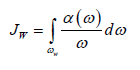 – the cumulative uptake of fashion
swinging for films а-Si:H и а-Ge:H. For specified films Aw=1,6∙1019
см-2 и Aw=1,1∙1019 сm-3, accordingly. Knowing NGe-H (where,
for films а-Ge:H, Aw=1,6∙1019 см-2 and α=5∙101 см-1), calculate
hydrogen concentration NH in the film а-Si1-xGex:H in the words of:
– the cumulative uptake of fashion
swinging for films а-Si:H и а-Ge:H. For specified films Aw=1,6∙1019
см-2 и Aw=1,1∙1019 сm-3, accordingly. Knowing NGe-H (where,
for films а-Ge:H, Aw=1,6∙1019 см-2 and α=5∙101 см-1), calculate
hydrogen concentration NH in the film а-Si1-xGex:H in the words of:

where is,  – number of links, some of the effects of net
swing а-Ge:H, the value which, calculated according to the equation
(5). The second factor in the expression for NH (cumulative ratio
of IR absorption maxima) is a vibrational fashion stretching in the
sample and in pure a-Ge: H. For the computation of the cumulative
ratio used maximum satisfying the oscillatory fashion stretching
Ge-H (2000 см-1) in the film а-Si1-xGex:H.
– number of links, some of the effects of net
swing а-Ge:H, the value which, calculated according to the equation
(5). The second factor in the expression for NH (cumulative ratio
of IR absorption maxima) is a vibrational fashion stretching in the
sample and in pure a-Ge: H. For the computation of the cumulative
ratio used maximum satisfying the oscillatory fashion stretching
Ge-H (2000 см-1) in the film а-Si1-xGex:H.
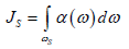
From these data it is possible to evaluate the effect of the oscillator in film а-Si1-xGex:H the ratio of: Q = JS/JW,
where is,  – are integrated acquisitions fashion, stretching and rocking,
accordingly. The oscillator strength Q= 0,51 (for х=0) и Г=0,13 (for
х=1). The maximum value Р=4,16 for х=0,40.
– are integrated acquisitions fashion, stretching and rocking,
accordingly. The oscillator strength Q= 0,51 (for х=0) и Г=0,13 (for
х=1). The maximum value Р=4,16 for х=0,40.
Table 1 shows the characteristic parameters of amorphous films а-Si0,60Ge 0,40:H. On Figure 2 shows the distribution of hydrogen on film thickness d: certain 1- method of recoil protons, 2- method of IR absorption spectrum. You can see, the distribution of hydrogen sufficiently uniform. Unlike other methods, the method of recoil protons (MOP) sample bombing beam of protons. When researching а-Si:H and its alloys, this allows you to get distribution hydrogen on thickness ~ 40 ÷ 100 Å. Method of calibration accuracy is limited only by the MCS, which is determined by the largest concentration of hydrogen (NH), and IR spectroscopy of found values that match 2 ÷ 3 %. This method provides information about the General content of both associated and not associated with Si hydrogen. А, with regard to the precise definition of hydrogen content in the volume of films, this band was analyzed INFRARED absorption 630 сm-1. To clarify the amount of hydrogen is embedded in amorphous matrix below as follows is determined by the structural parameter (R):
Table 1: Characteristic parameters of amorphous films a-Si0,60 Ge0,40 :H.


where is J2000 и J2100 – intensity of absorption bands at 2000 и 2100 см-1. Using the equation (3), of this ratio is determined by the concentration of hydrogen. Increase R occurs simultaneously with a decrease in the concentration of hydrogen. The highest magnitude R (before 0,8) observed for films а-Si:H, the besieged plasma chemical deposition method (ПХО), when TS=300 0С, power frequency discharge W=100W. However, the films studied in the present work, that when TS=200 ÷ 300 0С, micro structure parameter cannot vary in the range R= 0,1 ÷ 0,8. When annealing during 30 minutes in a vacuum at R value reaches 1.0. Accordingly, in this case, СH is 24.5 ÷ 14.0 at. %. By number of links Si-H, you can define a specific concentration of hydrogen containing links [Si–H]/[Si]. Specific concentrations of hydrogen containing Silicon links in the maximum reaches the value 0.58 [10–12].
Hydrogen concentration (NH), some effusion method, correlated with the concentration of hydrogen, calculated using the integrated force IW, fashion rocking 600 см-1 (рис. 3). The number of hydrogen atoms is found by at. % (СH), effusion method is defined for the data tapes and compared to the number of hydrogen atoms NА (Avogadro’s number).

- the film received when hydrogen pressure 0.6 mTorr.
- the film received when hydrogen pressure 1.2 mTorr.
- the film received when hydrogen pressure 1.8 mTorr.
- the film received at a pressure of hydrogen 2.4 mTorr.
- the film received when hydrogen pressure 3.0 mTorr.
Therefore, the ratio of  compared to СH (ат. %) (fig. 3). Change СH (at. %) for films at various temperatures heat up, shown
in the table 1. Found that after effusion, during heat treatment up to 650° c, hydrogen concentration is NH=1,3 ат. %. In doing so,
found that the strength of the oscillator depend Q on hydrogen
concentration (NH), It decreases after effusion of hydrogen;
with increased hydrogen content (РH2) in the atmosphere of the
received films а-Si0,60Ge0,40:H When partial pressures from 0.6
to 3.0 m Torr power oscillator increases [5, 12]. This is due to the
hydrogen containing links Ge:H, Si: H at specified frequency.
compared to СH (ат. %) (fig. 3). Change СH (at. %) for films at various temperatures heat up, shown
in the table 1. Found that after effusion, during heat treatment up to 650° c, hydrogen concentration is NH=1,3 ат. %. In doing so,
found that the strength of the oscillator depend Q on hydrogen
concentration (NH), It decreases after effusion of hydrogen;
with increased hydrogen content (РH2) in the atmosphere of the
received films а-Si0,60Ge0,40:H When partial pressures from 0.6
to 3.0 m Torr power oscillator increases [5, 12]. This is due to the
hydrogen containing links Ge:H, Si: H at specified frequency.
Heating the sample in a closed volume is due to the fact that the material almost completely decomposed into its constituent elements, with crystallization temperature range 350 ÷ 650 0С, what causes hydrogen jeffuziju and leads to increased pressure. Pressure measured capacitive pressure gauge with a precision of 0,1 %. To determine the effusion other gases should undertake quantitative mass spectrometric analysis of the composition of the gas. Note that the hydrogen inside the film identifies several ways: at. %,NH, РH2 and Р. To define these settings, you must remove the IR absorption spectra of the corresponding frequency fluctuations associated with the absorption of hydrogen.
Optical properties of thin films
The dependence of (αhν)1/2 from hν to determine the width of the forbidden zone [14, 16] for each film.
In all the studied films of the optical absorption edge ratio describes the ratio of:

where is, α = 5∙104 cm-1, E0 - optical band gap width for each film, В – the coefficient of proportionality. The value of the В determined by extrapolation of dependencies (αhν)1/2 from hν for each sample. Quadratic dependence (7) received in theory model [13,14], Describes the density of States slit mobility. The value of the В when х=0÷1 at. % Ge, for films а-Si1-xGex:H changes from 527 before 343 eV-1cm1/2, accordingly, E0=1,86 eV and E0=1,14 eV. Means with increasing content of Germany, E0 decreases. Mobility of carriers and photoconductivity in film а-Si1-xGex:H, also diminishes when Germany more 40 at.% [11, 12]. We use the known relative absorption coefficient α - is determined from the following equation [14 - 17]:

here take, that

For weakly absorbing light areas k20≤(n −1,5). к0 shows light attenuation in the substrate. Note that the film thickness d, defined in this case, the relevant transmission or reflection from extreme interference fringes.
From equation (8), the coefficients of absorption (α) are defined as follows:

Then,

Equation (11) is a working formula for determining optical absorption coefficients for films, in a weakly absorbing spectral region.
In a strongly absorbing spectral regions R3 = 0, R2 = R1 = R, n(λ ) = const and n = n1 =1,5 for glass substrates, а n = n1 = 3,42 for silicon substrate. Then equation (8) can be rewritten as follows:

then,

This formula can be used to determine the coefficient of optical absorption in a strongly absorbing spectral regions. Accordingly, the coefficients of refraction is defined using the following ratio:

or by using the following formula:

where is λm, λm-1 – the wavelength corresponding to the neigh bouring extreme and spectra of transparency or reflection (corresponding frequency, с- the speed of light. Refractive index is defined or the following formula [15]:

where is Tmax и Tmin – functions of the wavelength λ, n1 – index of refraction of the substrate, which is defined by the expression:

where is T1 – deletion of the substrate, which is almost always in the area of transparency. As for glass substrates T1 = 0,91, то n1= 1,554. Accordingly, the film thickness is calculated by the formula:

where is λ1 и λ2 – wavelengths which correspond to the neigh pouring extreme points on the spectrum bandwidth, А=1 for two extremes of the same type (max– max, min– min) and А=0,5 for two adjacent extremums of the opposite type (max– min, min– max).
Creation of solar cells
Studies show that films а-Si1-xGex:H (x≥0,20) can be used as a qualitative material in semiconductor electronics [12]. For this purpose, we have developed a 3-item based on two elements of cascade type. Three-layer element is made of 2-layer element consisting of two elements on the basis а-Si:H с p-i-n transition and p-i-n element with i- a layer of film а-Si0,88Ge0,12: H. The thickness i-layers to the top two transitions selected in such a way that respected the condition of equality of short-circuit current lower element. Short circuit current was about half the value for an element with a p-i-n transition. Idling voltage and short circuit current decreases with increasing number of superimposed layers. This way you can build multiple layers (create n-layer element). Note that for each item produced i-0.5 μm thick layer. The area of each element was 1.3 cm2. When receiving a three-layer solar cells must be respected uniform thickness and square to each element. Substrate material of steel and was chosen as the cover used ZrO2 with missing light 80%. Covering the same time playing the role of upper ZrO2 (front) of the contact. The thickness of the layers of a-Si:H p-and n-types was ~300 and 400Å, respectively. For alloying films number of В2Н6 and РН3 in gas mixtures changed within Alloy films in gas mixtures changed within 0.1 and 0.5%, respectively. After the deposition of amorphous semiconducting layers deposited by evaporation film ZrO2 thickness ~ 500 Å. The upper contacts used Ni/Ag, for lower-stainless steel substrate. Items covered source sunlight provided АМ-1 (100 mW/sm2). Short-circuit current for 3-layer elements was 8,5 mA/cm2, no-load voltage ~ 2,25 V, fill factor ~ 0,50 and CPA ~ 9,5% (рис.4). CPA for single-layer and double-layer element is 7% and 8.9%, respectively. The effectiveness of collecting media when different wavelengths is defined by the formula:

where is Jф(λ) – the photocurrent density (10 mA/cm2), N(λ) – the number of photons incident per unit surface per second, e- free media charge.
For elements with the structures of the short-circuit current is calculated in the supposition of a complete depletion of all layers, in the absence of direct bias. Thus, the short circuit current for the first, second, and third elements provides the following expressions:

where is, Wi, Wn, Wp field distribution inside the i, n, p layer, respectively, Nph – the number of photons incident on the surface of the elements, R – reflectivity film, α – absorption coefficient for each layer elements.
Idling voltage for cascading elements with two and three transitions is presented as:

The fill factor for all elements of the set size 0.5. Shortcircuit current of a cascading element with two sets of values less transitions Isc(II) sets the lower value Isc1 and Isc2 . Short-circuit current of a cascading element with three passages is determined by the smallest amount of Isc1, Isc2 or Isc3.
CPA of many transitional cascade elements is given by the expression:

where is i = 2 and 3 – shows the number of layers, Pin – power of incident light to the surface elements, its value is 100 mW/cm2, E01, E02, E03 – Accordingly, the width of the forbidden zone for each i- the layer.
To raise η for solar cell, you want to increase the number of layers reduce the area elements, the choice of metal wires to reduce the resistance of the metal contacts, etc. Measurement of spectral sensitivity is usually produced at a constant illumination with white light, the intensity of which corresponds to the normal conditions of work (AM-1~100 mW/cm2), at the same time an element falls modulation calibrated monochromatic radiation. Photocurrent and its dependence on wavelength of monochromatic radiation is measured in shorted circuits by using synchronized amplifier. To determine the effectiveness of collecting important knowledge of the electric field which is passed to the element. It has been noticed that in device dependently to the configuration collection efficiency is offset from red light in the blue spectrum. It is known that the photon energy and momentum of the corresponding electromagnetic wave with frequency and wavelength in vacuum, equal:

where is, h- Planck’s constant. When agile frequencies ν - the preponderant role played by wave properties, at large ν - particle properties of light. If P*- electromagnetic radiation energy feeding okay on some surface unit area for 1 sec, c-the speed of propagation of light waves in a vacuum, R-reflectivity surface pressure p-light on this surface as well:

light pressure (P) is defined by equation (20) and represent the following form:

N- the number of incident photons. W- photon energy falling at all wavelengths of the body surface. P* -momentum light falling on dies surface for 1 sec. Then the pressure of the incoming light is defined in the following form:

F - the power of light pressure (F=10-8 H) on the surface (S=1cm2), λ - incident wave length, t - time of incidence of the light for 1 sec. with energy P* and its value is Nhν photons, with the momentum of each photon is equal to hν/c. With radiation reflection R, λ- the number falling photon is 1017÷1018 м-2с-1, λ = 300 ÷ 900 nm (fig. 4).

Conclusion
Obtained thin films а-Si1-xGex:H (х=0÷1) plasma-chemical
deposition method using gas mixtures of H2 + SiH4; H2+GeH4 in
various proportions. It was determined that the highest R value (up
to 0.8) is observed for films of a-Si: H deposited method (PHO) at
temperature t = 300° c, with an output frequency of discharge W =
100 W. The data on the ratio of  The oscillator strength in the
film was evaluated а-Si1-xGex:H, где
The oscillator strength in the
film was evaluated а-Si1-xGex:H, где  Oscillator strength Q=0,51 (for х=0) and G=0,13 (for х=1). For
х=0,40 the maximum value Р=4,16.
Oscillator strength Q=0,51 (for х=0) and G=0,13 (for х=1). For
х=0,40 the maximum value Р=4,16.
Based on the films а-Si:H and а-Si0,88Ge0,12:H manufactured solar cells and created single-layer, double-layer and three-layer structure; their characteristics are measured. Found that for single-layer, double-layer and three-layer structures with an area element 1,3 cm2 η is 7 %; 8,9%; 9,5%, accordingly. For the three layered element highs move in the scope of collection efficiency of longer wavelengths. In the reporting structures of their light in the wavelength interval 0,3 ÷ 1,1 μm within 120 hours, there has been no degradation. It is shown that the multi-layer structure solar cells based on α-Si0,88Ge0,12:H and α-Si:H effective, and the improvement of their Efficiency are relevant tasks.
Acknowledgement
None.
Conflict of Interest
No Conflict of Interest.
References
- Wang Yan, Han Xiaoyan, Zhu Feng, Hou Guofu, Ren Huizhi (2006) J Non Cryst Solids 9(20): 1909-1912.
- K Shimazaki, M Imaizumi (2007) JAEA-Rev 42: 5.
- S Neretina, NV Sochinskii, PJ Mascher (2006) J Electron Mat 34(6): 786- 790.
- TJ Stanimirova, PA Atanasov, et al. (2007) J Appl Surface Sci 253(19): 8206-8209.
- Chen Chao, Liu Yu-zhen, Zhang Cuo-bin (2007) J Luminescence 28(4): 579-584.
- Matsui T, Ogata K, Isomura M, Kondo M (2006) J Non Crys Solids 352(9- 20): 1255-1258.
- BA Najafov (2016) Journal Fund. studies 7: 61-73.
- BA Najafov, VR Fiqarov (2010) International Journal of Hydrogen Energy 35: 4361-4367.
- Uchida Guchiro, Sato Muneharu, Seo Hyunwoong (2013) Thin Solid Films 544: 93-98.
- Sachenko, DV Korbutyak, Yu. Kryuchenko (2011) Nanoelectron and Opto electron 6(4): 420-426.
- BA Najafov, GI Isakov (2007) Alternative Energy and Ekol 11: 177-178.
- B Najafov, FP Abasov (2015) Optoelectronic thin film processes and prospects of application LAP, Germany. с. 433.
- VV. Beams, M Solovan, et al. (2014) FTT 56(10).
- BA Najafov, GI Isakov (2005) JPS 72(3): 371-376.
- BA Najafov, Gi Isakov (2010) Inorganic mat 46(6): 624-630.
- BA Najafov, FP Abasov (2014) Photonics, Ross 44(2): 72-90.
- BA Najafov (2016) Int. Journal of Applied and Fundamental Research 12: 1613-1617.
-

This work is licensed under a Creative Commons Attribution-NonCommercial 4.0 International License.