
 Review Article
Evidence of Electron Charging Induced Alternating Currents in Nanopillar Transistor
Received Date: June 06 , 2019; Published Date: June 10 , 2019
Abstract
Study of electron charging in nanopillar transistor at 300K shows that elastic vibration is an automatic behavior in the device. The frequency observed in the drain-source current is found to agree with the charging frequency. Given a quantum dot of size ~10x10x9nm3, the maximum displacement estimated is 0.3nm. Once the displacement diminishes to zero, single-electron tunnel dominates the I-V. A forced vibration model is proposed to explain the correlation between surface charges and vibrations. When the distribution of charges is uniformly on each SiNx atom, vibration becomes stable and can yield homogenous damping current.
Keywords:Quantum dot; Nanopillar transistor; Pulse voltage; Mechanical vibration
Introduction
Electron transport in electro-mechanical quantum dot transistors [1] has been a hot topic for more than three decades. No doubt it is very interesting for engineers as it has the potential to revolutionize semiconductor technology. The disclosure of single electron tunnel is definitely a hall mark effect because it can transform into the useful devices such as single-electron pump [2], single-electron memory cell [3] and single-electron detectors or counters [4]. Along with these works, we have presented “nanopillars” transistor [5]. In this device, the structure is in vertical form; drain current versus drain-source voltage measurements show excellent feature of single-electron charging. By matching the charging peaks with the parallel plate charging energy Ec = e2/2C, single electron effect is evident.
However, a critical issue remains unanswered is that the onset of peaks is not well defined. Early studies at low temperatures [6] found similar effect and it was attributed to the so-called “Coulomb blockade” where the first electron is blocked by Coulomb energy and no electrical current is allowed to move. But recently, quantum shuttle [7] was proposed to deliberate that at finite temperatures electrons could move from one electrode to another electrode via the repetitive motion of the central quantum dot. Consequently, current noises [8] appear. In this highly unstable region, mechanisms of mechanical dissipation [9], elastic deformation and electro-mechanical feedback [10] can stand out and play vital roles. As such, it definitely worth to do carefully experiments in this region. As expected, we find that at low charging voltages, the I-V does show drastically different behavior. What observed are giant current oscillations from the very beginning. After reaching a peak the current decreases quickly to zero. To understand these effects, a forced vibration model is proposed to explain the data and good agreements are found.
Device
The transistor, schematically drawn in Figure 1, was fabricated on p-type (100) silicon wafers. It basically features a center silicon separated from the top and bottom contacts by two nitride barriers. This dot cavity has a critical length of 3 nm and is intimately coupled to a gate electrode on the side. The device was then loaded into a probe station (Thermal Cascade) for current-voltage measurements. HP 4156 C three-terminal meter was used. It had the resolution of 1mV and 10 fA. Since our model is intimately related to the manner of electrical charging, in Figure 2(a), the pulsed voltages are schematically drawn. Within the time period of 1mS, 1mV was first applied on the first half cycle. After that another 1mV was added to the 1mV for a total of 2mV on the device in the next period.

Theoretical Model
This kind of charging is commonly known by experimentalists as it can avoid overheating. In Figure 2(b), when certain amounts of charges Qs are accumulated on the surface of the bottom nitride layer, it will create a force to bend the layers. On the other end of the layers, a positive current +I(t) is produced. The elasticity of all layers, here marked as energy ΔE, then will force a backward movement moment later to create a negative current –I(t). As a consequence, alternating currents appear. Correspondingly, displacement x(t) will change between +α and –α as illustrated in Figure 2(c).


The best model for such behavior is the dynamical equation 𝑚ẍ(t)+cẋ(t)+kx(t)=f(t) [11], where ẍ(t) is the second order time derivative of x(t); ẋ(t) is the first order derivative; x(t) is the displacement; m represents the mass of the system as shown in Figure 3, c denotes the damping coefficient, k is the spring constant and f(t) is the applied force.
To solve this equation, two conditions must be considered.
One is the zero-force f(t)=0 case and the other is the finite force
case, f(t)>0. The solution xg(𝑡) is a textbook example and it is  whereα is the maximum displacement, 𝜉 is the
ratio
whereα is the maximum displacement, 𝜉 is the
ratio 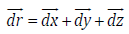 is the nature frequency.
Inside the bracket of the sinusoidal function
is the nature frequency.
Inside the bracket of the sinusoidal function  response frequency. With this identity, one can calculate the current.
Note that Ig(t)= neAυd where n is the volume density of electrons, A
is layer area, υd is the drift velocity as defined by ẋ(t). Given all the
parameters, the current created by the damping vibration is found
to be
response frequency. With this identity, one can calculate the current.
Note that Ig(t)= neAυd where n is the volume density of electrons, A
is layer area, υd is the drift velocity as defined by ẋ(t). Given all the
parameters, the current created by the damping vibration is found
to be

Other than the homogeneous current of Ig(t), there is the particular current Ip(t). Derivation of it is different from the Ig(t) and that it is discussed in reference [12]. Once the theoretical derivation is finished, the data is fitted and compared.
Data Analysis
In Figure 4(a), a Ig(t) curve is plotted in the window of 0 – 0.25 s for comparison to the data. This result is obtained by several tries on the ω and the ξ which appear to be the most critical parameters in the model. Notice that these alternating current mimics the main features of the data in the bottom figure very well. In Figure 4(b), the good fitting comes from the range between 0 and 0.17 V where a smaller damping and a slightly higher ω appears to dominate the whole spectrum. After the ac damping, the transistor becomes stable and single electron tunnel appears and dominates the transport. This analysis answers the key query of this paper and also proves that mechanical stability is an essential part for the upcoming quantum tunnel of electrons.

Acknowledgement
None.
Conflict of Interest
No conflict of interest.
References
- Park H, Park J, Lim AK, Anderson EH, Alivisatos AP, et al. (2000) Nanomechanical oscillations in a single-C60 transistor. Nature (London) 407: 57-60.
- Y Ono, Y Takahasi (2003) Electron pump by a combined single-electron/ field-effect- transistor structure. Appl Phys Lett 82(8): 1221.
- NJ Stone, H Ahmed (2004) Appl Phys Lett 84: 4632.
- Wei Wu, Jian Gu, Haixiong Ge, Christopher Keimel, Stephen Y Chou (2003) Room-temperature si single-electron memory fabricated by nanoimprint lithography. Appl Phys Lett 83(11): 2268.
- Yue Min Wan, Pei Ming Yang, Che Ming Yang, Hsiang Chen Hsu (2005) Nano spot analysis on nanopillar transistor for room temperature application. Appl Phys Lett 87: 1.
- (1992) Single Charge Tunneling, edited by H Grabert, MH Devoret, Plenum Press, New York.
- KB Fournier, C Constantin, J Poco, MC Miller, CA Back, et al. (2004) Efficient Multi-keV X-Ray Sources from Ti-Doped Aerogel Targets. Phys Rev Lett 92(16): 165005.
- A Donarini, T Novotny, AP Jauho (2004) Simple models suffice for the single dot quantum shuttle. Phys Rev Lett 92: 1-24.
- N Nishiguchi (2003) Elastic deformation blockade in a single-electron transistor. Phys Rev B 68(12): 121305.
- Ya M Blanter (2004) Phys Rev Lett 93: 136802.
- (1996) Theory of Vibration, edited by AA Shabana, 2nd edition (Springer- Verlag, New York).
- Te Chien Wang, Yue Min Wan (2017) Chin J Phys 55: 1225.
-

This work is licensed under a Creative Commons Attribution-NonCommercial 4.0 International License.