 Mini Review
Two-Dimensional MoS2 and Heterostructure Growth by Pulsed Laser Deposition
Rajib Sahu, Max Planck Institute for Iron Research, Düsseldorf 40237, Germany.
Received Date: November 18, 2019; Published Date: November 27, 2019
Introduction
Due to having zero band gap in two-dimensional graphene shifted the attention towards MoS2, WS2, and similar inorganic transition metal-based dichalcogenides. Most of them perform indirect to direct band gap crossover form bulk to monolayer make them a potential candidate for optoelectronic device applications [1-4]. MoS2 is stabilized in 2H semiconducting state, having a band gap of 1.9 eV for monolayer and 1.28 eV for bulk [5-6]. Thinnest transistor based on MoS2 have been already reported [2]. Based on unique excitons, spin and valley properties, MoS2 is considered for the next-generation platform for future electronics [7-9]. The metastable 1T phase is demanding due to metallicity and shows excellent hydrogen evolution activity [10-12]. This qualitative metal-semiconducting state in 1T-2H phase transition is promising for switchable device applications [13-14].
Mechanically exfoliated and chemically synthesized TMDCs are investigated primarily for fundamental properties are not suitable for large area practical devices [15-16]. Bottom-up synthesis, namely chemical vapor synthesis (CVD), molecular beam epitaxy (MBE), metal-organic chemical vapor deposition (MOCVD), and magnetron sputtering (MS), pulsed laser deposition (PLD) are significantly successful producing scalable high quality MoS2 thin film. However, the challenges for researchers in theses growth methods include contaminations, choice of precursor, proper precursor transport and controlled chemical reactions, formation of byproducts, growth kinetics for layered control synthesis, time, and cost. For instant MoS2 growth in CVD has proven to be a versatile method. Still, the yield is low, and contamination is moderate due to sluggish thermal evaporation and chemical reactions of desired precursors [17]. The restriction of the choice of growth substrate is limited due to high substrate temperature [18]. Similarly, MOCVD uses metal organic gasses like (C2H5)2S and Mo (CO)6 for chemical reactions and forms high chemical contaminations level [19]. MBE method is highly cost-effective for ultra-high vacuum and finds time consuming [20-21]. The most challenging issue is the limitation of substrate choice due to lattice miss-match between film and substrates. We find magnetron sputtering is simple, clean, scalable, low time consuming and low-cost effective but suffer from poor crystal quality, rough surface, high energy consumption [22- 23]. Therefore, we look forward for a simple, fast, low cost, highly controllable, scalable, and less contaminated universal growth solution (Figure 1).
PLD has several advantages over other growth techniques and potentially competent to address all the issues as mentioned earlier. PLD is simple, highly manageable, clean, safe, highly efficient, easily controllable, scalable and versatile method. Generally, the method includes a high vacuum growth chamber, gas flow, optical path and a high energy excimer laser. In first step, pulsed laser is focused on the target and starts bombarding the surface. Then, the generating plasma plume is deposited on a substrate placed on the heater inside the chamber. One can easily optimize the growth kinetics controlling mentioned parameters; laser energy, laser pulse rate, laser pulse width, substrate temperature, gas flow, pressure, targetsubstrate distance, target composition and thickness. Therefore, two-dimensional (2D) graphene, MoS2 and other inorganic TMDCs are successfully synthesized using PLD.

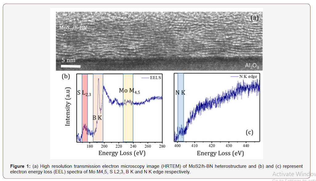
In 2015, Serrao et al. reported MoS2 deposition on several substrates; Al2O3 (0001), GaN (0001) and SiC-6H (0001) by PLD [24]. Serna et al. successfully deposited stoichiometric scalable MoS2 films without additional surface preparation of the substrate [25]. Our findings show under slow kinetics provide precise control on the thickness of MoS2 down to 1ML [26]. Challenges are initially to optimize growth conditions result buckling of MoS2 layers and form a polycrystalline film. We solved this issue keeping the nucleation temperature at 400°C with laser ablation frequency of 1 Hz. We observe only nucleation temperature are different for other TMDCs, but slow kinetics works well to keep Van der waal layers intact with underlying substrate forms crystalline film. Now, one could think one step further growing heterostructure in PLD. MoS2 based multilayered heterostructures have been reported for optical and magnetic applications [27-28]. Our HRTEM image shows scalable MoS2/h-BN heterostructure on c-plane sapphire in Figure 1(a). High resolution electron energy loss spectra confirm chemical identification of the heterostructure (Figure 1(b) & (c)).
Conclusion
In summary, we briefly review the growth method of MoS2 and MoS2 based heterostructures. PLD is much effective and significant among all simple and fast TMDCs based growth techniques. PLD is a promising method to transfer stoichiometric transfer of starting materials to substrate. Improvement of PLD day by day makes it versatile method. Now challenges one can think further to grow horizontal heterostructures inside PLD chamber.
Acknowledgement
None.
Conflict of Interest
No conflict of interest.
References
- Wang HQ, Kalantar-Zadesh K, Kis A, Coleman JN, Strano MS (2012) Electronics and optoelectronics of two dimentional transition metal dichalcogenides. Nature Nanotechnology 7: 699-712.
- Radisavljevic B, Radenovic A, Brivio J, Giacometti, Kis A (2011) Single-layer MoS2 Nature Nanotechnology 6: 147-150.
- Jariwala D, Sangwan VK, Lauhon LJ, Marks TJ, Hersam MC (2014) Emerging device applications for semiconducting two-dimensional transition dichalcogenides. ACS Nano 8(2): 1102-1120.
- Xu M, Liang T, Shi M, Chen H (2013) Graphene-like two dimensional materials. Chem Rev 113(5): 3766-3798.
- Mak KF, Lee C, Hone J, Shan J, Heinz TF (2010) Atomically thin MoS2: a new direct-gap semiconductor. Physical review letter 105(13): 136805.
- Dileep K, Sahu R, Peter SC, Datta R (2016) Layer specific optical band gap measurement at nanoscale in MoS2 and ReS2 Vander waals compounds by high resolution electron energy loss spectroscopy. Journal of Applied Physics 119: 114309.
- Tizei L, Lin Y, Mukai M, Sawada H, Lu A, et al. (2015) Exciton Mapping at Subwavelength Scales in Two-Dimensional Materials. Physical review letter 114: 107601.
- Roch JG, Froehlicher G, Leisgang N, Makk P, Watanabe K, et al. (2019) Spin-polarized electrons in monolayer MoS2. Nature Nanotechnology 14(5): 432-436.
- Xiao D, Liu G, Feng W, Xu X, Yao W (2012) Coupled Spin and Valley Physics in Monolayers of MoS2 and Other Group-VI Dichalcogenides. Physical review letter 108: 196802.
- Lukowski MA, Daniel AS, Meng F, Forticaus A, Li L, et al. (2013) Enhanced Hydrogen Evolution Catalysis from Chemically Exfoliated Metallic MoS2 Nanosheets. J Am Chem Soc 135(28): 10274-10277.
- Voiry D, Salehi M, Silva R, Fujita T, Chen M, et al. (2013) Conducting MoS2 Nanosheets as Catalysts for Hydrogen Evolution Reaction. Nano Lett 13(12): 6222-6227.
- Yu Y, Nam G, He Q, Wu X, Zhang K, et al. (2018) High phase-purity 1T′-MoS2- and 1T′-MoSe2-layered crystals. Nature Chemistry 10(6): 638-643.
- Sahu R, Bhat U, Batra N, Sharona H, Vishal B, et al. (2017) Nature of low dimensional structural modulations and relative phase stability in RexMo(W)1-xS2 transition metal dichalcogenide alloys. Journal of Applied Physics 121(10): 105101.
- Chou SS, Huang Y, Kim J, Kaehr B, Foley BM, et al. (2015) Controlling the Metal to Semiconductor Transition of MoS2 and WS2 in Solution. J Am Chem Soc 137(5): 1742-1745.
- Matte HS, Gomathi A, Manna AK, Late DJ, Datta R, et al. (2010) MoS2 and WS2 Analogues of Graphene. Angew Chem Int Ed Engl 49(24): 4059-4062.
- Liu N, Kim P, Kim J, Ye J, Kim S, et al. (2014) Large-Area Atomically Thin MoS2 Nanosheets Prepared Using Electrochemical Exfoliation. ACS Nano 8(7): 6902-6910.
- Liu HF, Wong SL, Chi DZ (2015) Growth of MoS2‐based Two‐dimensional Materials. Chemical Vapor Deposition 21(10‐11‐12): 241‐259.
- Lee YH, Zhang XQ, Zhang W, Chang MT, Lin CT, et al. (2012) Synthesis of large-area MoS2 atomic layers with chemical vapor deposition. Adv Mater 24(17): 2320-2325.
- Briggs N, Subramanian S, Lin Z, Li X, Zhang X, et al. (2019) A roadmap for electronic grade 2D materials. 2D materials 6(2): 022001.
- Roy A, Movva HCP, Satpati, B, Kim K, Dey R, et al. (2016) Structural and electrical properties of MoTe2 and MoSe2 grown by molecular beam epitaxy. ACS Appl. Mater. Interfaces 8(11): 7396-7402.
- Zhan L, Wan W, Zhu Z, Shih TM, Cai W (2017) MoS2 materials synthesized on SiO2/Si substrates via MBE. Journal of Physics: Conference series 864: 012037.
- Ling ZP, Yang R, Chai JW, Wang SJ, Leong WS, et al. (2015) Large-scale two-dimensional MoS2 photodetectors by magnetron sputtering. Optic Express 23(10): 13580-13586.
- Tao J, Chai J, Lu X, Wong LM, Wong TI, et al. (2015) Growth of wafer-scale MoS2 monolayer by magnetron sputtering. Nanoscale 7(6): 2497-2503.
- Serrao CR, Diamond AM, Hsu S, You L, Gadgil S, et al. (2015) Highly crystalline MoS2 thin films grown by pulsed laser deposition. Applied Physics Letter 106:
- Serna MI, Yoo SH, Moreno S, Xi Y, Oviedo Jp, et al. (2016) Large-Area Deposition of MoS2 by Pulsed Laser Deposition with In Situ Thickness Control. ACS Nano 10(6): 6054-6061.
- Sahu R, Radhakrishnan D, Vishal B, Negi DS, Sil A, et al. (2017) Substrate induced tuning of compressive strain and phonon modes in large area MoS2 and WS2 van der Waals epitaxial thin films. Journal of Crystal Growth 470: 51-57.
- Bhat U, Singh R, Vishal B, Sharma A, Horta S, et al. (2018) Distinct Photoluminescence in Multilayered van der Waals Heterostructures of MoS2/WS2/ReS2 and BN. Physica status solidi b 255(7): 1700691.
- Jie W, Yang Z, Zhang F, Bai G, Leung Cw, et al. (2017) Observation of Room-Temperature Magnetoresistance in Monolayer MoS2 by Ferromagnetic Gating. ACS Nano 11(7): 6950-6958.
-
Rajib Sahu. Two-Dimensional MoS2 and Heterostructure Growth by Pulsed Laser Deposition. Mod Concept Material Sci. 2(2): 2019. MCMS.MS.ID.000534.
-
2D TMDCs, MoS2, Heterostructure, PLD, Laser Deposition, Growth
-

This work is licensed under a Creative Commons Attribution-NonCommercial 4.0 International License.


