 Research Article
Optimized Design of the 100-V Silicon Based Power N-Channel LDMOS Transistor
Shen Li Chen* and SP Lee
Department of Electronic Engineering, National United University, Taiwan
Shen Li Chen, Department of Electronic Engineering, National United University, 2, Lien-Da Rd, Miaoli City 36063, Taiwan.
Received Date: July 02, 2020; Published Date: July 21, 2020
Abstract
In power integrated circuits (PICs), it is desirable to minimize the area of a power device region while maximizing its performances (i.e., higher breakdown voltage and lower on-resistance). Therefore, the area of a power device region mainly determines the total chip size and hence the cost. An optimized design of breakdown voltage and on-resistance in a power n-channel lateral-diffused MOSFET (nLDMOS) was investigated in this paper. Two-dimensional process and device simulators, such as the TSUPREM4 and Sentaurus EDA tools, will be used to predict the device characteristic behaviors. Eventually, it can be shown that a 100 V device will have an optimized breakdown voltage about 156.7 volts and onresistance Ron about 40.61 mΩ-cm2 under the Vgs-Vth= 5 V and LOCOS spacing d= 6 μm situations.
Keywords: Breakdown voltage; High Voltage (HV); Local Oxidation of Silicon (LOCOS); N-channel lateral-diffused MOSFET (nLDMOS); Onresistance
Introduction
A lateral double-diffused MOSFET (LDMOS) component has been widely used in smart power ICs, lighting, automotive system, and 5G communication applications [1-8]. It is with the advantage of its process compatible to VLSI process and easy to integrate with other CMOS devices. Consequently, it is very important to improve its electrical performance by optimizing their breakdown voltage and on-resistance. A cost effective and elegant method to utilize such a trade-off between on-resistance and breakdown voltage is to optimize the device physical dimension design.
For an n-channel LDMOS structure, the device is operated with a high positive voltage applied to the drain end. When the gate electrode is short-circuited to the source side, the device can support a large drain voltage across the P-base/N-drift layer junction. The breakdown voltage is dependent not only on the device structure, but also is affected by the physical dimension design of this device [9-15].
Meanwhile, when a positive bias is applied to the gate electrode, the surface channel of nLDMOS becomes conductive. At a low drain voltage, the current flow is essentially resistive, with the on-resistance determined by the sum of the source, channel, drift region, and drain-end resistances. The channel resistance decreases with increasing a gate bias, whereas the source/drain and drift region resistances remain a constant. Then, the total onresistance decreases with increasing a gate bias until it approaches a constant value. Under a large gate bias voltage, the channel resistance becomes smaller than that of the drift region resistance, and the device on-resistance becomes independent of gate bias. The total on-resistance is a measure of the current handling capability of the device because it determines the power dissipation during the current conduction. The on-resistance is defined as the slope of output characteristics in the linear region at low drain voltages. Furthermore, the on-resistance parameter is an important power MOSFET parameter in circuit designs.
Device Structure
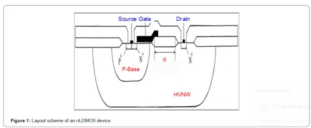
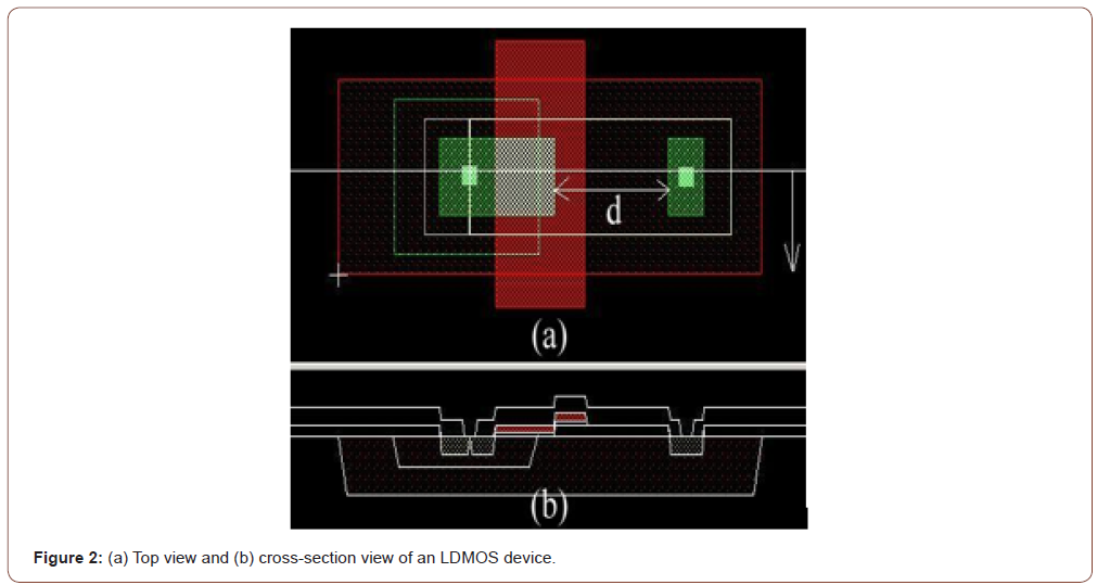
Figure 1 shows the cross-section structure scheme of an LDMOS device, meanwhile, the top view of layout design and the corresponding cross-section of an LDMOS are presented in Figure 2. For a high-voltage LDMOS component, a field-oxide layer is fabricated near the drain side and used to improve the breakdown voltage. However, the Ron increased significantly due to an extra current path underneath this region. Then, in order to improve the Ron resistance [16-24], this LOCOS extra current path should be reduced. Unfortunately, by reducing the extra current path, the drain peak field is too close to the gate edge and the breakdown voltage will be significantly reduced.
In this paper, an optimized spacing distance underneath the field oxide dependence of high performance in the 100 V nLDMOS based on numerical simulators such as TSUPREM4 and Sentaurus will be investigated.
Process Simulation in an NLDMOS
The explored devices were processed by using a 100 V BCD process, and process simulations were performed by the TSUPREM4 simulator [25]. One part of the cross-section diagram for an LDMOS device based on simulator is shown in Figure 3.
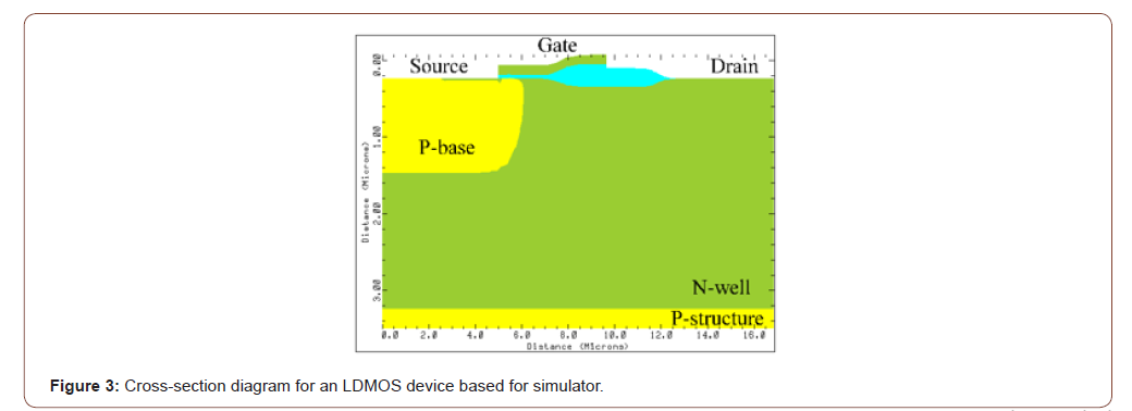
A p-type substrate with σ= 15~25 Ω-cm is selected, and an HV N-well serves as the drift region. In the following process, phosphorus and boron ions were implanted into the HV N-well and P-base regions, respectively. And, then a high temperature process was executed and used to drive-in. Eventually, the field oxide thickness was set to be 6000 Å. The gate oxide thickness was 400 Å formed by a thermal SiO2 layer; an n+ polysilicon with 1250 Å thickness was used to as the gate electrode; and source/drain regions were fabricated by implanting arsenic atoms. Finally, the detailed process information is listed in Table 1.
Table 1:Process parameters of an nLDMOS device.
Device Simulation in an NLDMOS
The two-dimensional numerical device simulator Sentaurus [26] is used to predict the device performance of nLDMOS devices. Here, the 2-D device simulator Sentaurus with TSUPREM4 resultant impurity data as the import file was used; the Sentaurus program solves the Poisson and continuity equations by numerical methods.
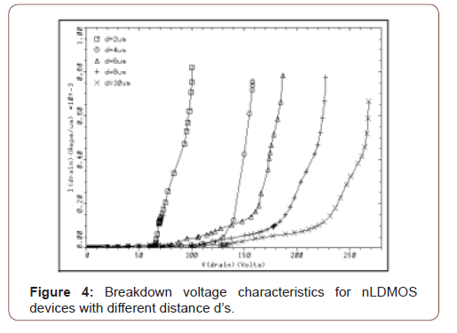
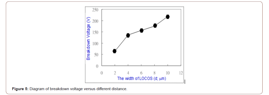
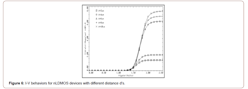
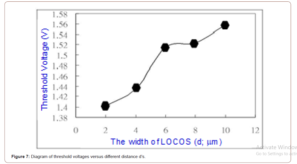
The breakdown voltage capability that is functioned of the distance d underneath the field oxide is shown in Figure 4 and 5. As expected, the breakdown voltage is increased with a longer distance d. Figure 6 and 7 are the plot of devices threshold voltages with different distance d’s. It is shown that the threshold voltage slightly decreased with the decreasing distance d value. Finally, the simulated Ron for nLDMOS devices with various distance d’s under a Vgs-Vth= 5V biased condition is illustrated in Figure 8 and 9. Increasing LOCOS spacing d, therefore, the current flow path increasing, an extra current path resulted in higher breakdown voltage and on-resistance values. Therefore, a “figure of merit (FOM)” index is defined as

Then, the FOM values versus different distance d’s can be shown in Figure 10, as an nLDMOS is fabricated with a 6-μm spacing width underneath the field oxide, which provides a maximized FOM value in which the corresponding breakdown voltage is 156.7 V and on-resistance under the Vgs-Vth= 5V condition is 40.61mΩ-cm2. Therefore, the d= 6-μm spacing width is a best receipt in this 100 V nLDMOS fabrication by the LOCOS spacing adjustment.


Conclusion
A high performance power device is essential for power integrated circuits. However, the simulation is an essential tool in the optimization of a complicated high-voltage MOSFET design. A combination of 2-D process and device simulations has been used to design and optimize the fabrication of a 100V n-channel lateraldiffused MOSFET (nLDMOS) device for high voltage applications. A high performance nLDMOS device has been proposed and achieved in this paper. A spacing “d” underneath the field oxide will affect the breakdown voltage and on-resistance eventually. Finally, when an nLDMOS is fabricated with a 6-μm LOCOS spacing underneath the field oxide, it provides a best condition in electrical behaviors, in which the breakdown voltage is 156.7V and on-resistance under the Vgs-Vth= 5V biased condition is 40.61 mΩ-cm2.
Acknowledgement
In this paper, authors would like to thank the Taiwan Semiconductor Research Institute in Taiwan for providing the process information and fabrication platform. And, authors would like to acknowledge the financial support of the Ministry of Science & Technology of Taiwan.
Conflict of Interest
No conflict of interest.
References
- F Lepine, A Adahl, H Zirath (2005) L-band LDMOS power amplifiers based on an inverse class-F architecture. IEEE Trans on Microwave Theory and Techniques 53(6): 2007-2012.
- D Gruner, R Sorge, O Bengtsson, AA Tanany, G Boeck (2010) Analysis, Design, and Evaluation of LDMOS FETs for RF Power Applications up to 6 GHz. IEEE Trans on Microwave Theory and Techniques 58(12): 4022-4030.
- Y Chen, C Chang, P Yang (2015) A Novel Primary-Side Controlled Universal-Input AC–DC LED Driver Based on a Source-Driving Control Scheme. IEEE Trans on Power Electronics 30(8): 4327-4335.
- C Chang, T Jiang, P Yang, Y Xu, C Xu, et al. (2017) Adaptive line voltage compensation scheme for a source-driving controlled AC–DC LED driver. IET Circuits Devices & Systems 11(1): 21-28.
- JI Matsuda, A Kuwana, JY Kojima, N Tsukiji, H Kobayashi (2018) 14th IEEE International Conference on Solid-State and Integrated Circuit Technology (ICSSICT): 1-3.
- G Bosi, A Raffo, F Trevisan, V Vadalà, G Crupi, et al. (2018) Nonlinear-Embedding Design Methodology Oriented to LDMOS Power Amplifiers. IEEE Trans on Power Electronics 33(10): 8764-8774.
- WA Malik, WM Abdulkawi, AA Sheta, NF Alzakari (2019) 16th International Bhurban Conference on Applied Sciences and Technology (IBCAST): 1053-1056.
- C Zhang, H Guo, Z Chen, W Yue, Y Li, et al. (2020) Super Field Plate Technique That Can Provide Charge Balance Effect for Lateral Power Devices Without Occupying Drift Region. IEEE Trans on Electron Devices 67(5): 2218-2222.
- E Napoli (2007) Duration of the High Breakdown Voltage Phase in Deep Depletion SOI LDMOS. IEEE Electron Device Letters 28(8): 753-755.
- Z Wang, B Zhang, Q Fu, G Xie, Z Li (2012) An L-Shaped Trench SOI-LDMOS With Vertical and Lateral Dielectric Field Enhancement. IEEE Electron Device Letters 33(5): 703-705.
- MH Han, HB Chen, CJ Chang, CC Tsai, CY Chang (2013) Improving Breakdown Voltage of LDMOS Using a Novel Cost Effective Design. IEEE Trans on Semiconductor Manufacturing 26(2): 248-252.
- X Luo, J Wei, X Shi, K Zhou, R Tian, et al. (2014) Novel Reduced ON-Resistance LDMOS With an Enhanced Breakdown Voltage. IEEE Trans. on Electron Devices 61(12): 4304-4308.
- K Zhou, X Luo, Z Li, B Zhang (2015) Analytical Model and New Structure of the Variable- k Dielectric Trench LDMOS With Improved Breakdown Voltage and Specific ON-Resistance. IEEE Trans. on Electron Devices 62(10): 3334-3340.
- M Mehrad, M Zareiee, AA Orouji (2017) Controlled Kink Effect in a Novel High-Voltage LDMOS Transistor by Creating Local Minimum in Energy Band Diagram. IEEE Trans. on Electron Devices 64(10): 4213-4218.
- K Yang, Y Guo, J Zhang, J Yao, M Li, et al. (2020) An Analytical Breakdown Model for the SOI LDMOS With Arbitrary Drift Doping Profile by Using Effective Substrate Voltage Method. IEEE Journal of the Electron Devices Society 8: 49-56.
- R Menozzi, AC Kingswood (2005) A new technique to measure the thermal resistance of LDMOS transistors. IEEE Trans on Device and Materials Reliability 5(3): 515-521.
- JS Yuan, L Jiang (2008) Evaluation of Hot-Electron Effect on LDMOS Device and Circuit Performances. IEEE Trans on Electron Devices 55(6): 1519-1523
- B Zhang, W Wang, W Chen, Z Li, Z Li (2009) High-Voltage LDMOS With Charge-Balanced Surface Low On-Resistance Path Layer. IEEE Electron Device Letters 30(8): 849-851.
- FJ Yang, J Gong, RY Su, KH Huo, CL Tsai, et al. (2013) A 700-V Device in High-Voltage Power ICs With Low On-State Resistance and Enhanced SOA. IEEE Trans on Electron Devices 60(9): 2847-2853.
- X Luo, J Wei, X Shi, K Zhou, R Tian, et al. (2014) Novel Reduced ON-Resistance LDMOS With an Enhanced Breakdown Voltage. IEEE Trans on Electron Devices 61(12): 4304-4308.
- M Qiao, Z Wang, Y Wang, L Yu, Q Xiao, et al. (2017) 3-D Edge Termination Design and RON,sp -BV Model of A 700-V Triple RESURF LDMOS With N-Type Top Layer. IEEE Trans on Electron Devices 64(6): 2579-2586.
- B Yi, J Cheng, XB Chen (2018) A High-Voltage “Quasi-p-LDMOS” Using Electrons as Carriers in Drift Region Applied for SPIC. IEEE Trans on Power Electronics 33(4): 3363-3374.
- S Chahar, GM Rather, N Hakim (2019) The Effect of Shallow Trench Isolation and Sinker on the Performance of Dual-Gate LDMOS Device. IEEE Trans on Electron Devices 66(1): 585-591.
- R Ye, L Lu, S Liu, H Wu, H Chen, et al. (2020) Reliability Concerns on LDMOS With Different Split-STI Layout Patterns. IEEE Trans on Electron Devices 67(1): 185- 192.
- (2017) Taurus™ TSUPREM-4™ User Guide. Version N-2017.09, Synopsys.
- (2015) Sentaurus™ Device User Guide Version K-2015.06, Synopsys.
-
Shen Li Chen, SP Lee. Optimized Design of the 100-V Silicon Based Power N-Channel LDMOS Transistor. Mod Concept Material Sci. 3(2): 2020. MCMS. MS.ID.000559.
-
Breakdown voltage, High Voltage (HV), Local Oxidation of Silicon (LOCOS), N-channel lateral-diffused MOSFET (nLDMOS), On-resistance, Electrode, Simulator, Gate bias, Circuit, Field oxide
-

This work is licensed under a Creative Commons Attribution-NonCommercial 4.0 International License.


