 Short Communication
Influence of SiC consumption on SiC MOSFET electrical parameter
Dario Tenaglia* and Massimo Davide Pirnaci
STMicroelectronics, Zona Industriale Stradale Primosole, 50 – 95121 Catania, Italy
Dario Tenaglia, STMicroelectronics, Zona Industriale Stradale Primosole, 50 – 95121 Catania, Italy
Received Date:October 01, 2025; Published Date:October 13, 2025
Introduction
In the manufacturing of SiC power devices the definition of some specific areas known like Body (NBL) and Source (SOU) is critical for the electrical behavior, in this area of the device the socalled “channel” is defined by ion implantation, the consumption of the SiC during the etch can affect the electrical field modifying the depth of the implanted area. The process of ion implantation is a critical step in the fabrication of various SiC devices, as it enables wide-range doping control for both n- and p-type conductivity [1]. Etching process has been optimized on SiC 8” in terms of selectivity with the substrate improving the chemistry of the etch recipe.
Table 1: Elastic Moduli of α-Quartz (trigonal with 6 independent Young’s moduli from Crystran’s Handbook at 106; 87; 58; -18, 13; 7 GPa, where C means stiffness = compliance C11=87 C12=7 C44=58 C13=13 C14= (−)18 C33=106 are the ultimate data from RUS (relaxation ultrasound spectroscopy).

Experimental
4H-SiC 200mm substrates have been selected for the fabrication of MOSFET devices on SiC. TEOS layer, used as mask for the ion implantation, was deposited by a PE-CVD process on the top of the SiC wafer. Photoresist film was deposited by spin-coating technique on the top of the surface. Then, the pattern of the photoresist film was performed by a photolithographic process. The opening of the TEOS was performed by a plasma etching process in an ICP reactor chamber [2]. After the TEOS etching, the residual portions of the photoresist were totally removed.
Plasma based on CF4, CHF3 or C4F8 assisted by O2 and Ar are widely used for etching oxide layers, the selectivity of the dry etching process with SiC is critical for some specific applications, addition of CO in the gas mixture improved the selectivity by reducing the SiC consumption.
Morphological Characterization
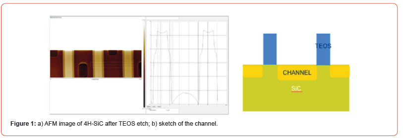
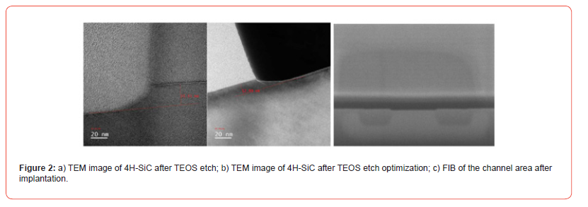
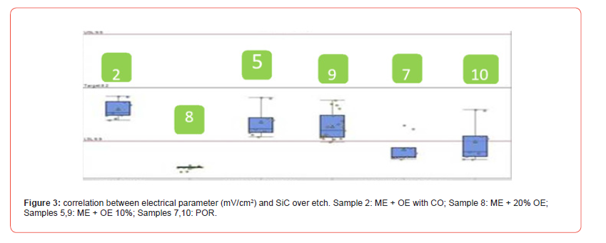
From AFM and TEM analysis, it is possible to detect the consumption of SiC. The parametric test shows the correlation between the consumption and the electrical parameter.
The over etch of the SiC can be tuned by the recipe used for the TEOS dry etch process, the next picture 3 shows the improvement in terms of consumption and electrical behavior related to the process condition of the over etch step.


Conclusion
Relevant contribution of the CO is detected by TEM, with the std process the SiC consumption was ~ 25nm, after the optimization of the over etch is ~ 13nm. Parametric test confirms the effect of the over etch in a specific area of the device because of the depth reached by the ion implantation (channel).
Electrical specification related to the electrical field can be achieved improving the selectivity with SiC at the TEOS dry etch.
References
- Maurizio Di Paolo Emilio (2024) SiC Technology Materials, Manufacturing, Devices and Design for Power Conversion.
- Jerome Biscarrat, Jean-François Michaud, Emmanuel Collard, Daniel Alquier (2013) ICP etching of 4H-SiC substrates, Materials Science Forum 740: 825-828.
-
Dario Tenaglia* and Massimo Davide Pirnaci. Influence of SiC consumption on SiC MOSFET electrical parameter. Mod Concept Material Sci. 7(4): 2025. MCMS. MS.ID.000667.
-
Indentation, Physical-Stiffness, Compliance, Modulus, Loading-Curve, Polymorphs, Basic- Errors, Faulty-Unloading, Steepness, Berkovich, Differentiation, Linearity, Multiple-Errors, Correctness, Iterations, Side-Face
-

This work is licensed under a Creative Commons Attribution-NonCommercial 4.0 International License.


