 Research article
A Modified Quadratic Boost Converter with Reduced Voltage Stress on the Output Capacitor
Maryam Tarighat Monfared and Hossein Gholizadeh*
Electrical Engineering Faculty, Shahid Beheshti University, Tehran, Iran
Hossein Gholizadeh, Electrical Engineering Faculty Shahid Beheshti University, Tehran, Iran.
Received Date:January 23, 2023; Published Date:February 07, 2023
Abstract
In this paper, a quadratic boost converter has been introduced. Besides the converter’s high voltage ratio compared with the conventional converters, a low number of magnetic elements have been used in this converter. Moreover, combining all capacitors’ voltage provided its output voltage. Therefore, the voltage stress of the output capacitor has decreased. Moreover, the input voltage plays a direct role in the output voltage. It is good to mention that this converter has been discussed in both continuous/discontinuous conduction modes. Moreover, the converter’s behavior has been discussed in both ideal and nonideal modes. Finally, the simulation results have been extracted by PLECS and compared with the theoretical relations and assumptions.
Keywords:Boost topology; High voltage ratio; Quadratic, boost converters
Introduction
The main idea of the converters is to get more efficiency and reliability in many portable devices [1]. These DC-DC converters can be categorized into isolated and non-isolated [2]. The popular isolated converters are half/bridge, fly-back, and forward topologies. The turn ratio of the high-frequency coils provides a high voltage gain by the mentioned type of converters. However, many downsides of the isolated converters, such as the dramatic high cost, mass, volume, and current/ voltage stress of the switch, limit the employment of these converters [3]. Moreover, the leakage inductance of the transformers is an issue in these topologies [4,5]. Therefore, to eliminate the caused downsides, the non-dissipative snubbers are applied to the topologies. However, such a solution raises the size, and the control process becomes complex. The non-isolated conventional converters are boost, buckboost, buck, Cuk, and SEPIC converters [6]. Notably, the traditional reported topologies are not an appropriate selection for high voltage gain provides. Moreover, employing the highduty cycle percentages to provide higher orders of voltage gain forces the semiconductor’s high current/voltage stresses [7]. Furthermore, the duty cycle’s high percentages conclude a poor efficiency. Therefore, the resulting voltage ratio is unacceptable due to the low efficiency [8]. Such concepts provide the fields to offer new topologies of non-isolated converters to provide higher voltage gain than conventional structures [9,10] recommends a quadratic buck-boost converter. Three inductors/capacitors beside two switches/diodes have made it a 10-element DC-DC topology. The converter’s voltage gain is the quadratic form of the buck-boost voltage gain. Therefore, it cannot provide a low duty cycle percentage of high voltage gain. It is good to mention that employing the duty cycle high percentages lead to semiconductors’ high current/voltage stresses and poor efficiency. In addition, the higher number of components has not provided the desired voltage gain. Furthermore, the converter’s topology has different MOSFETs that lead to different drive circuits. Notably, the continuity of the output current has been provided by an inductor which has increased the volume of the converter. [11] introduces another structure of the quadratic buck-boost converters. Like the previous topology, it has ten elements. Its voltage gain cannot provide a higher value due to the low percentage of the duty cycle. Moreover, the output capacitor experiences a dramatic high current stress due to discontinuous output current. In [12], another quadratic buck-boost converter has been proposed. Notably, the number of components has decreased compared to the topologies discussed. However, both input and output currents are discontinuous in this converter. Therefore, high current stress is forced on both input/output filter capacitors. It is good to mention that the employed MOSFETs are not the same-typed. Consequently, the driving circuit becomes different and increases the complexity.
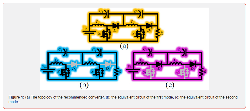
In this paper, a quadratic boost converter has been recommended. It is good to mention that the proposed converter has 8 circuit elements. Therefore, the low number of components provides a higher voltage ratio. Additionally, this converter can increase its input voltage to 4 times higher than the output capacitor. However, the converter’s voltage gain in [10]-[12] concludes unity, while the duty cycle percentage becomes 50 percent. All capacitors act as the converter’s output filter in the proposed converter. Moreover, the converter’s input voltage directly makes a part of the output voltage besides the capacitors. Therefore, the voltage stresses of capacitors decrease. Both the switches in the converter are the same typed. Moreover, both are low-sided switches that lead to a simple drive circuit (Figure 1).
The Study of the Proposed Converter in Ideal and Continuous Current Mode
In this paper, a high-gain DC-DC converter has been introduced, which consists of two inductors, two switches, and two capacitors. The distinctive feature of this converter is that the input voltage is directly involved in providing the output voltage. Moreover, what is considered the output filter capacitor are both capacitors of this converter which help each other to make the output voltage gradually. Therefore, using a large capacitor in the output terminal is not necessary. Such an explanation is the main difference between the proposed topology and the cascaded connection of the boost converters. The used components’ low numbers and high voltage ratio, which has achieved a high value compared with the traditional converter, are the other bold features of this converter. Additionally, some assumptions have been considered to describe the converter: (i) All elements are assumed to be ideal. Moreover, the converter is operating in the continuous current mode. In addition, the inductors are highvalued that the converter remains in CCM. (ii) The capacitors’ voltage is constant due to the capacitance sufficiency. The circuit of the designed converter is shown in Figure 1(a). As shown in Figure 1 (b) and Figure 1 (c), this circuit has two operating modes in CCM. According to Figure 1 (b), both switches are activated, and the diodes become inactivated. The input voltage is applied to the first inductor, and the sum of the input voltage and the first capacitor voltage is applied to the second inductor. In addition, the inductors’ voltage is positive. Consequently, they become magnetized. Additionally, due to the cross of currents from the negative terminal of the capacitors, they have become discharged. During the second mode, the first and second inductors’ voltage is the first and second capacitors’ voltage, respectively. In this case, their negative voltage demagnetized them. Additionally, the inductors’ current charges the capacitors. Therefore, their crossing current is positive. (1) reports the functional equations of this topology (Figure 2).
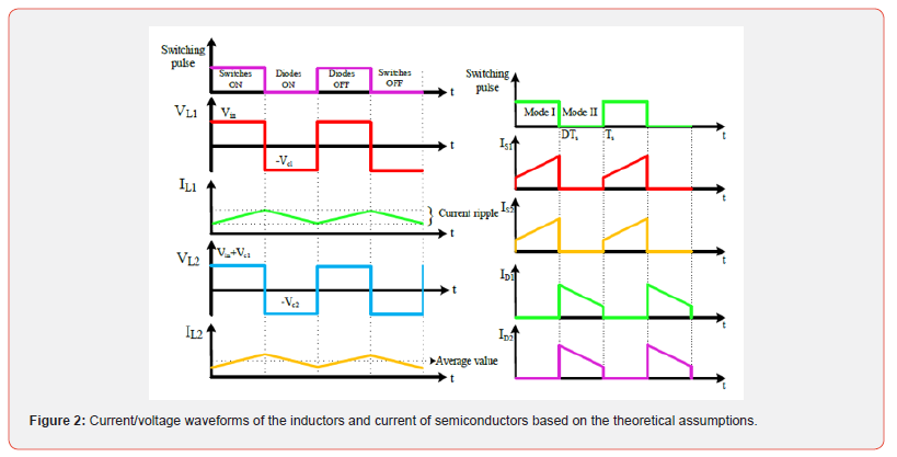

In the steady state, the capacitors’ average current and inductors’ average voltage are zero. In this case, the written relations in (1) equal zero. Consequently, (2) presents the capacitors’ average voltage and inductors’ average current.

According to the explained voltage gain, the voltage gain has a quadratic format. Such a characteristic causes a sharp voltage gain rise as the duty cycle increases. (3) reports the semiconductors’ voltage/current stresses according to Figure 2.

Furthermore, the capacitor voltage ripple and the inductors current ripple are as (4).

Discontinuous Conduction Mode
The extracted relations in section 2 are mainly related to CCM. In addition, DCM is caused by two factors, 1) The inductor value and 2) The inductors’ average current. The inductors’ value affects the inductors’ current ripple. Therefore, by decreasing the inductors’ value, their current ripple rises. When the inductor current ripple value is more than twice the average inductor current, the converter is in DCM. Therefore, the minimum value of the inductors is calculated as (5) (Figure 3-5).
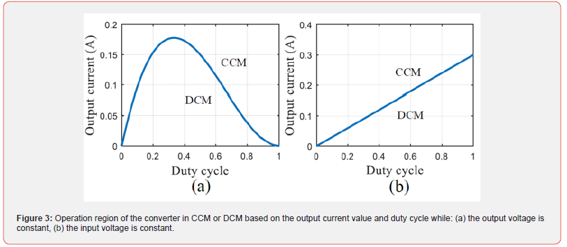

The output current average value influences the inductors’ average current. Therefore, when the average output current is lower than a particular value, the converter switches to DCM. In other words, when the average inductors’ current is less than their current ripple half, the converter operates in its DCM. Consequently, the output current concerning the duty cycle value has defined the converter’s operating region in CCM and DCM in Figure 3. (6) reports the appropriate relations which conclude the mentioned figure.

Figure 3(a) is according to the first part of (6) as well as the second part with Figure 3(b). (7) reports the appropriate voltage gain of the converter in DCM.

The Expressing Voltage Gain of the Non-Ideal Mode
All the expressed concepts in the second section are in the ideal state. Albeit, in the experiment setup, the circuit elements are non-ideal. Therefore, the non-ideal voltage gain differs from what was obtained in section 2. (8) describes the nonideal voltage gain considering the resistance of the inductors, switches, and diodes.

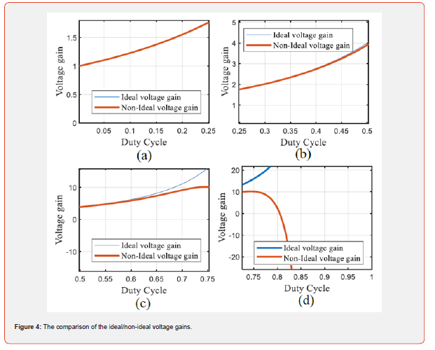
It is worth noting that rL,rS, rD, and R correspond to the parasitic resistance of inductors, switches, diodes, and load value, respectively. Figure 4 compares the ideal/non-ideal voltage gain according to this relation. According to Figure. 4 (a)-(c), when the duty cycle varies from zero to 65 %, the ideal/nonideal gains are approximately the same. When the duty cycle is more than 65 %, the ideal-ideal gain differences increase.
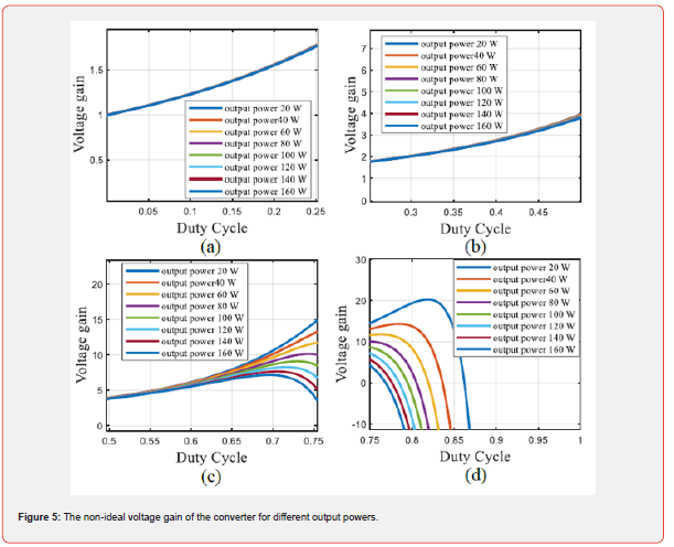
Based on Figure (d), a 75 % duty cycle provides the maximum voltage gain. In addition, the voltage gain decreases for the rest of the interval in the non-ideal mode. According to the described relation in (6), the quality of the components and the output power influence the voltage gain. Figure 5 presents the converter’s voltage gain for the various output powers. Based on Figure 5 (a)-(c), when the duty cycle is from 0 to 60 %, the non-ideal voltage gain is the same for the various output powers. On the contrary, when the duty cycle is more than 60 %, the difference in voltage gain behavior for different output powers increases. As the output power value increases, the voltage gain maximum, and its corresponding duty cycle decreases.
Efficiency
In this section, considering the component’s conduction loss along with the frequency loss of the switches and excluding the hysteresiscurrent loss and diodes’ frequency loss, the converter efficiency is as (9).

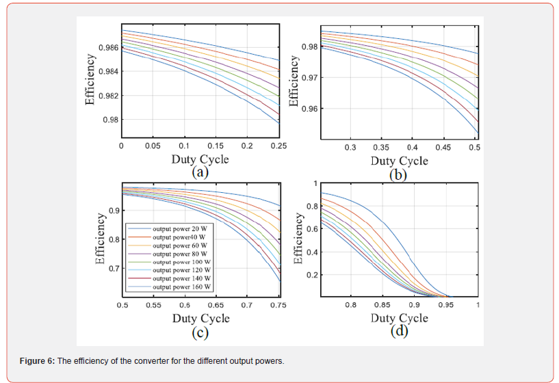
Based on this relation, output power, and components quality influence efficiency. Figure 6(a)-(d) shows converter efficiency for various output powers. Based on Figure 6(a)- (c), varying duty cycle from 0 to 62 %, concludes converter efficiencies of more than 90 % for all the mentioned output powers. Furthermore, as the duty cycle percentage is less than 68 percent, the efficiency remains more than 90 % for the output powers of less than 80 W. Moreover, according to Figure 6(d), when the duty cycle approaches 80 percent, the efficiency decreases for all output power values.
The Comparison of the Proposed Converter with the Recently Suggested Topologies
Tables. I and II compare the voltage/current stress of the semiconductors and different kinds of power losses. The output power is 80 W during the comparison. Moreover, the reported duty cycle value for each converter in both tables provides a 4-times voltage gain. The reported duty cycle for the proposed one has the lowest value. According to Table. I, the normalized semiconductors’ voltage/ current stress in the proposed converter, have achieved the lowest value compared with [10]-[12]. Additionally, according to Table. II, the switch’s conduction loss in the recommended topology has the lowest value. It is good to mention that the diode loss of the recommended topology is higher than the rest. According to the last column of the second Table, the proposed topology has achieved the highest efficiency compared to others.
Table 1:Comparison of Voltage/Current Stresses.
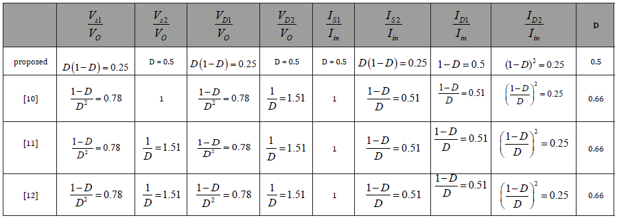
Table 2:Comparison of Power Loss.
The Comparison of the Proposed Converter with the Recently Suggested Topologies
Tables. I and II compare the voltage/current stress of the semiconductors and different kinds of power losses. The output power is 80 W during the comparison. Moreover, the reported duty cycle value for each converter in both tables provides a 4-times voltage gain. The reported duty cycle for the proposed one has the lowest value. According to Table. I, the normalized semiconductors’ voltage/ current stress in the proposed converter, have achieved the lowest value compared with [10]-[12]. Additionally, according to Table. II, the switch’s conduction loss in the recommended topology has the lowest value. It is good to mention that the diode loss of the recommended topology is higher than the rest. According to the last column of the second Table, the proposed topology has achieved the highest efficiency compared to others.
Small-Signal Analysis
The small-signal analysis has been held here to study the converter’s controlling concepts. The space state matrices must be found to find the controlling concepts of the converter. Notably, the inductors’ current and capacitors’ voltage have been considered state variables. (10) expresses the space state equations of the proposed topology.

(11) shows the matrix form of the space state equation.
Simulation Outcomes
The simulation results have been extracted in this section to determine the correctness of the extracted relations. In addition, to simulate the converter of this article, PLECS software has been used. The version of the used one was 4.1.2. The voltage/current ripples are required to find the inductors’ and capacitors’ values. It is good to mention that some quantities in the mentioned relations must be quantified. Therefore, some assumptions have been considered. The input voltage is 20 V, the switching frequency is 100 KH, the percentage of the inductors’ current ripple is 30 percent, the percentage of the capacitors’ voltage ripple is 5 percent, and the output current is 1A. (12) describes the energy-storing components.

Figure 7 presents the simulation results. All components’ voltage/ current waveforms have been extracted. (13) reports the capacitors’ average voltage and inductors’ average current according to the extracted results (Table 1 and 2, Figure 6, 7).

Comparing these extracted values with the design assumptions defines the correctness of the extracted relations. Furthermore, the inductors’ average voltage and capacitors’ average current are zero according to the simulation results.
Figure 7 presents semiconductors’ current/voltage waveforms. According to this figure, the extracted values and the predicted values in the second section are compatible with each other.

Conclusion
In this paper, a quadratic boost converter was proposed. Besides its higher voltage gain in comparison with conventional stepup converters, the output voltage was provided by all capacitors and input sources directly. It is good to mention that this feature decreased the voltage stress of the output capacitor. Moreover, the capacitors and input source provide the output current. The topology was discussed in both CCM/DCM. Furthermore, the converter’s behavior was studied in both the ideal/non-ideal modes. The voltage gain and efficiency were also discussed for the different output power values. The last section reported and compared the simulation results with the theory. The compatibility of the extracted values concluded the correctness of the extracted theoretical relations besides its correct operation.
Acknowledgement
None.
Conflict of Interest
No conflict of interest.
References
- S Hasanpour, M Forouzesh, YP Siwakoti (2021) Full Soft-Switching Ultra-High Gain DC/DC Converter Using Three-Winding Coupled- Inductor,” 2021 12th Power Electronics, Drive Systems, and Technologies Conference (PEDSTC): pp. 1-7.
- P Mohseni, S Rahimpour, M Dezhbord, MR Islam, KM Muttaqi (2020) “An Optimal Structure for High Step-Up Non-Isolated DCDC Converters with Soft-Switching Capability and Zero Input Current Ripple,” in IEEE Transactions on Industrial Electronics.
- Abbasi M, Abbasi E, Li L (2021) New transformer-less DC–DC converter topologies with reduced voltage stress on capacitors and increased voltage conversion ratio. IET Power Electron 14: 1173– 1192.
- Lotfi Nejad M, Poorali B, Adib E, Motie Birjandi AA (2016) New cascade boost converter with reduced losses. IET Power Electronics 9: 1213-1219.
- Abid R (2017) Comparative study of the performances of the DC/DC luo-converter in photovoltaic applications.” 2017 International Conference on Smart, Monitored and Controlled Cities (SM2C): 117-122.
- Amir A, Amir A, Che HS, Elkhateb A, Abd Rahim N (2019) Comparative analysis of high voltage gain DC-DC converter topologies for photovoltaic systems. Renew. Energy 136: 1147–1163.
- Tewari N, Sreedevi V (2018) A novel single switch DC-DC converter with high voltage gain capability for solar PV based power generation systems. Sol. Energy 171: 466–477.
- Revathi BS, Prabhakar M (2016) Non isolated high gain DC-DC converter topologies for PV applications—A comprehensive review. Renew. Sustain. Energy Rev 66: 920-933.
- Taghvaee M, Radzi M, Moosavain S, Hizam H, Marhaban MH (2013) A current and future study on non-isolated DC–DC converters for photovoltaic applications. Renew. Sustain. Energy Rev 17: 216–227.
- Gholizadeh, A. Sarikhani and M. Hamzeh (2019) A Transformerless Quadratic Buck-Boost Converter Suitable for Renewable Applications,” 2019 10th International Power Electronics, Drive Systems and Technologies Conference (PEDSTC), Shiraz, Iran, pp. 470-474.
- H Gholizadeh, M Salehi, Z Rafiee, E Afjei, M Hamzeh (2020) ”A Transformer less Quadratic Buck-Boost Converter with Wide Range of Output Voltage and Low Switch Stresses,” 2020 11th Power Electronics, Drive Systems, and Technologies Conference (PEDSTC): pp. 1-6.
- S Miao, F Wang, X Ma (2016) ”A New Transformerless Buck–Boost Converter With Positive Output Voltage,” in IEEE Transactions on Industrial Electronics 63(5): 2965-2975.
-
Maryam Tarighat Monfared and Hossein Gholizadeh*. A Modified Quadratic Boost Converter with Reduced Voltage Stress on the Output Capacitor. On Journ of Robotics & Autom. 1(5): 2023. OJRAT.MS.ID.000521.
Electrical Engineering, Quadratic, Voltage Stress, Output Capacitor, Boost topology; High voltage ratio; Quadratic, boost converters.
-

This work is licensed under a Creative Commons Attribution-NonCommercial 4.0 International License.


