 Mini Review
Growth Study of Silicon Nanowires Synthesized Via Plasma-Assisted VLS Using Tin Catalysts
Siham Djoumi1*, Fatiha Kail1, Pere Roca i Cabarrocas2 and Larbi Chahed1
1LPCMME, University Oran1, Algeria
2LPICM, Ecole Polytechnique, University Paris-Saclay, France
Siham Djoumi, LPCMME, University Oran1, BP1524, El M’naouar 31100 Oran, Algeria.
Received Date: January 21, 2020; Published Date: February 12, 2020
Abstract
In the present work, silicon nanowires (SiNWs) have been grown on crystalline silicon (Si) (100) oriented and hydrogenated amorphous silicon a-Si:H coated c-Si (a-Si: H/c-Si) substrates by plasma-enhanced chemical vapor deposition (PECVD) via the vapor-liquid-solid (VLS) process at different temperature. Tin (Sn) catalyst coating with a thickness of 1 nm were used as metal catalysts. A hydrogen plasma was applied to reduce the oxide and to form Sn droplets. SiNWs were then grown by introducing pure silane (SiH4) into the reactor with a flow rate of 5 sccm and a chamber pressure of 1.33 mbar, at a substrate temperature between 400 and 600°C. Their morphological and surface characteristics have been investigated using Hitachi S4800 scanning electron microscopy (SEM). Morphology obtained from SEM shows tapered growth of NWs with a distinctively sharp tip.
Keywords: Silicon nanowires SiNWs; Plasma enhanced chemical vapor deposition (PECVD); Tin (Sn) catalyst
Introduction
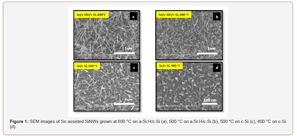
Si nanowires (NWs) have attracted extraordinary attention recently because of their unique mechanical, electrical, and optical properties. Particularly, SiNWs are highly desirable for new generations of electronic and photonic devices such as transistors [1], memory [2], biosensors [3], solar cells [4-5], and battery electrodes [6]. To date, many approaches have been developed to synthesize SiNWs, such as laser ablation metal-catalytic method [7,8], molecular beam epitaxy (MBE) [9], thermal vapor deposition [10], chemical vapor deposition (CVD) is one of the most common methods used to grow SiNWs [11] and plasma enhanced chemical vapor deposition (PECVD) [12]. The nanowires which are prepared by CVD method are grown via the Vapor-Liquid-Solid (VLS) proposed by Wagner and Ellis [13]. VLS offers great flexibility in the choice of catalysts [14]. Gold (Au) seed particle is the material most commonly used as a catalyst for the synthesis of SiNWs due to its high chemical stability, its lack of toxicity and its eutectic point at about 19% Si is relatively low [15] and can be deposited easily. Silicon atoms resulting from the decomposition of vaporphase source materials such as silane (SiH4) are absorbed by the Au nanoparticles. The absorbed Si atoms and the Au nanoparticles form an alloy (Au-Si) in the form of liquid droplet at the growth temperature. Si precipitates onto the substrate when the liquid alloy reaches super-saturation to form SiNWs. At the same time, it has several disadvantages such as when used for Si nanowires growth, it imposes deep level impurity that significantly degrades the electronic and optical properties [16,17]. It is for this reason that an alternative metal to gold has been investigated for the synthesis of semiconductor NWs. From this point of view, Tin can be used as an alternative candidate because of its low eutectic point (232 °C) and low solubility in Si. Thin films of the Sn catalyst, with 1 nm of thickness, were prepared by the thermal evaporation method at a pressure of 2×10⁻⁶ mbar vacuum on crystalline (100) silicon wafer c-Si and hydrogenated amorphous silicon coated c-Si a-Si:H/ c-Si substrates at room temperature. The samples were loaded into PECVD chamber, Sn nanoparticles were formed by exposure to 100 sccm of H2 plasma for 2 min, SiNWs were then grown for 20 min by introducing pure silane (SiH4) into the reactor with a flow rate of 5 sccm at a substrate temperature between 400 and 600 °C. SEMs showing that the Tin catalyzed SiNWs are tapered in nature and randomly oriented. The density and the morphology of the NWs are influenced by the growth temperature and by the substrate.

Acknowledgement
None.
Conflict of Interest
No conflict of interest.
References
- Zhong ZH, Fang Y, Lu W, Lieber CM (2005) Coherent single charge transport in molecular-scale silicon nanowires. Nano Lett 5(6): 1143-1146.
- Parkin SSP, Hayashi M, Thomas L (2008) Magnetic domain-wall racetrack memory. Science 320(5873): 190-194.
- Cui Y, Wei QQ, Park HK, Lieber CM (2001) Nanowire nanosensors for highly sensitive and selective detection of biological and chemical species. Science 293(5533): 1289-1292.
- Vardi A et al (2006) Room temperature demonstration of GaN/AlN quantum dot intraband infrared photodetector at fiber-optics communication wavelength. Appl Phys Lett 88(14): 143101.
- L Yu, F Fortuna, B O’Donnell, T Jeon, M Foldyna, et al. (2012) Bismuth-Catalyzed and Doped Silicon Nanowires for One-Pump-Down Fabrication of Radial Junction Solar Cells. NanoLett 12(8): 4153-4158.
- Law M, Greene LE, Johnson JC, Saykally R, Yang PD (2005) Nanowire dye-sensitized solar cells. Nat Mater 4(6): 455-459.
- AM Morales, CM Lieber (1998) A Laser Ablation Method for the Synthesis of Crystalline Semiconductor Nanowires. Science 279(5348): 208-211.
- YF Zhang, YH Tang, N Wang, DP Yu, CS Lee, et al. (1998) Silicon nanowires prepared by laser ablation at high temperature. Appl Phys Lett 72: 1835.
- Y Wu, R Fan, P Yang (2002) Block-by-block growth of single-crystalline Si/SiGe superlattice nanowires. Nano Lett 2(2): 83-86.
- YF Zhang, YH Tang, C Lam, N Wang, CS Lee, et al. (2000) Bulk-quantity Si nanowires synthesized by SiO sublimation. J Cryst Growth 212(1-2): 115-118.
- V Schmidt, JV Wittemann, S Senz, U Gosele (2009) Silicon Nanowires: A Review on Aspects of their Growth and their Electrical Properties. Adv Mater 21(25-26): 2681-2702.
- S Hofmann, C Ducati, RJ Neill, S Piscanec, AC Ferrari, et al. (2003) Gold catalyzed growth of silicon nanowires by plasma enhanced chemical vapor deposition. J Appl Phys 94: 6005-6012.
- Wagner RS, Ellis WC (1964) Synthesis and Characterization of GaN Rods Prepared by Ammono-Chemical Vapor Deposition. Appl Phys Lett 4(89): 89-90.
- Arbiol J, Kalache B, Roca i Cabarrocas P, Morante JR, Fontcuberta i Morral A (2007) Influence of Cu as a catalyst on the properties of silicon nanowires synthesized by the vapour–solid–solid mechanism. Nanotechnology 18: 305606.
- V Schmidt, JV Wittemann, S Senz, U. Gosele, Advanced Materials 21 (2009) 2681-2702.
- T Kamins (2007) Semiconductor nanowires for electronics and sensors, in WE-Heraeus Semin. Semiconducting Nanowires: Physics Materials and Devices, vol. 397.
- TI Kamins, RS Williams, Y Chen, YL Chang, YA Chang (2000) Chemical vapor deposition of Si nanowires nucleated by TiSi2 islands on Si. Appl Phys Lett 76: 562-564.
-
Siham D, Fatiha K, Pere Roca i C, Larbi C. Growth Study of Silicon Nanowires Synthesized Via Plasma-Assisted VLS Using Tin Catalysts. Mod Concept Material Sci. 2(5): 2020. MCMS.MS.ID.000546.
-
Silicon nanowires SiNWs, Plasma enhanced chemical vapor deposition (PECVD), Tin (Sn) catalyst, Plasma, Growth temperature, Substrate
-

This work is licensed under a Creative Commons Attribution-NonCommercial 4.0 International License.


