 Research Article
EKC Cleaning Effectiveness vs Fluorine
M Boscaglia, I Lopez Garcia, M Pirnaci, R Ricciari and D Tenaglia*
STMicroelectronics, Stradale Primosole Catania, Italy
D Tenaglia, STMicroelectronics, Stradale Primosole Catania, Italy.
Received Date:September 01, 2025; Published Date: September 18, 2025
Abstract
The utilization of EKC265 in semiconductor fabrication is critical for the effective removal of metal-organic polymers generated during dry etching processes with photoresist masks. This study investigates the efficacy of EKC265 in reducing surface fluorine (F) concentrations, as determined by X-ray Photoelectron Spectroscopy (XPS), on silicon carbide (SiC) power MOSFET devices.
Introduction
Manufacturing power MOSFET devices includes several steps, the pattern is reported on the surface of different materials with lithography processing, the definition of the structures is made by etching process through photoresist layer [1]. Especially in the dry etch the interaction between plasma, resist and exposed material makes polymers, in presence of metal exposed the EKC cleaning is necessary to remove the polymers.
Methodology
EKC265, contains hydroxylamine that is an extremely strong nucleophile that can attack the carbonyl groups of the polymer leading to its dissolution. Moreover, chelant agents are present in the solution, allowing the metallic species to removal.
The efficiency of the hydroxylamine to reduce the fluoride content is demonstrated by our experiment. The reduction of fluoride content via EKC265 was evaluated through XPS, a surface-sensitive analytical technique. XPS measurements were conducted using a PHI GENESIS 900 ULVAC-PHI spectrometer equipped with dual neutralizers (electron and ion) to ensure accurate surface characterization [2].
Experiment
The trials have been done on MOSFET device built on SiC 4H substrate. Silicon nitride used as passivation layer is deposited on AlSiCu pad, the passivation layer is defined by std litho-etch processes. The etch step is performed by plasma based on fluoride, the process leaves trace of fluoride on the material exposed to the plasma, under certain environmental conditions F can be combined, for example with the air humidity, forming HF which can cause the metal corrosion.
The resist stripping, performed by O2 plasma, is not effective on the F content, further cleaning with EKC265 is necessary.


Results
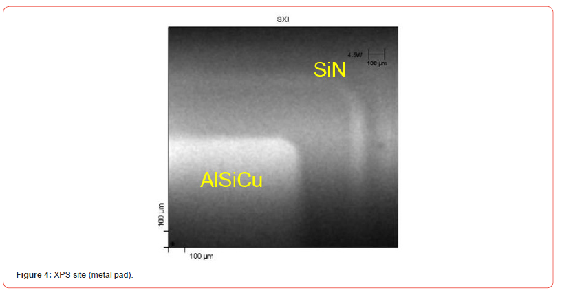
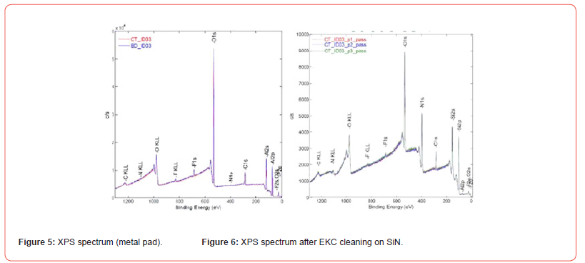
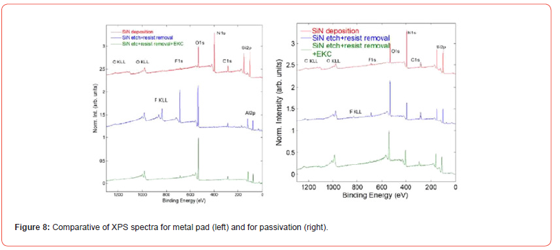
A small amount of F is detected by XPS even after the nitride deposition, then the analysis performed on two areas of the device, metal and passivation, show some differences related to the process steps.
Table 1:XPS after SiN deposition.

Table 2:XPS after SiN etch + resist removal.

Table 3: Some Applications of Elastic Modulus E, as used for Mechanical Properties of all Solid Materials, Including Viscoelastics with Modulus E instead of EphysXPS after SiN etch + resist removal + EKC.

Atomic percentage (%at.) refers to the relative proportion of a specific element within a sample, expressed as a percentage of the total number of atoms present. This measurement is used to quantify the elemental composition of the surface of a material.
XPS provided quantitative insights into the elemental composition of device surfaces, with atomic percentage (%at.) calculations reflecting the relative abundance of specific elements. The results achieved on the AlSiCu surface show a relevant decrease in the F content after EKC treatment.
Provocation Test to Induce Metal Corrotion Under Fluorine Presence
The formation of hydrofluoric (HF) can occur in the presence of fluorine (F2) and water vapor (H2O) under certain conditions.
The chemical reaction that describes this process is:

The reaction is exothermic and can occurs easily at room temperature. However, the reaction rate increases with rising temperature. At 85^C and with a water vapor concentration of 85%, it is likely that the reaction will occur, producing hydrofluoric acid (HF).
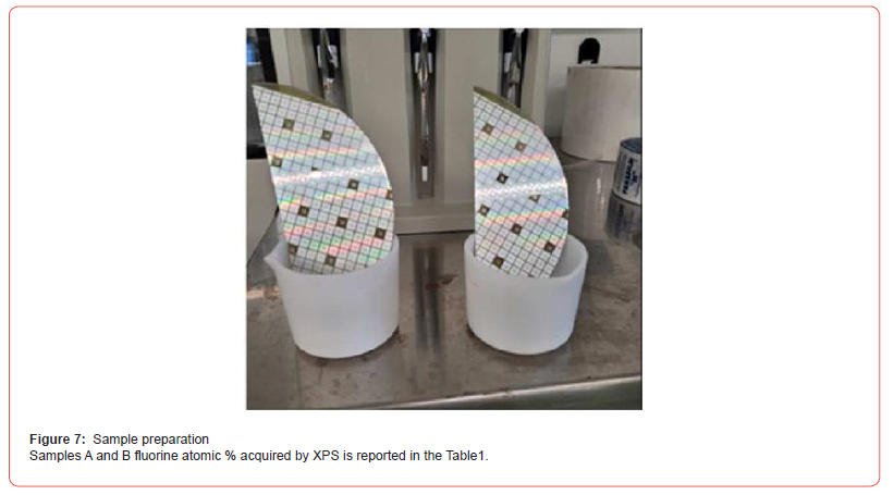
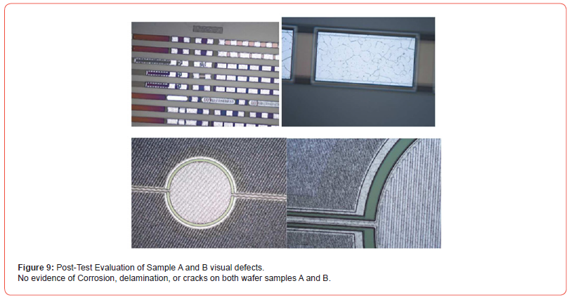
To evaluate the residual risk of metal oxidation and/or corrosion in the FAB process flow (see Pict. x, Scheme of passivation defined by litho-etch), two different wafer samples, A and B, were submitted to the 85/85 Humidity Test.
Appendix
85/85 test, 85% relative humidity (RH) and 85°C for 24 hours, is widely used in the semiconductor and electronics industries to evaluate the durability and reliability of materials, coatings, or devices under harsh environmental conditions.
Purpose of the 85/85 Humidity Test:
1. Moisture Resistance: To assess how well the wafer or its components
resist moisture ingress, which can cause corrosion,
delamination, or electrical failures.
2. Thermal Stress: To evaluate how materials or devices perform
under elevated temperature and humidity conditions.
3. Adhesion Testing: To check the stability of layers, coatings, or
bonds on the wafer.
4. Reliability Testing: To simulate long-term exposure to harsh
environments and predict the lifespan of the wafer or device.
Key Effects of the Test:
1. Oxidation or Corrosion:
o If the wafer has exposed metal layers (e.g., copper or aluminum),
moisture can lead to oxidation or corrosion, especially in
the presence of ionic contaminants.
2. Delamination:
o Moisture can weaken the adhesion between different layers
(e.g., passivation, dielectric, or metal layers), causing delamination
or cracking.
3. Electrical Failures:
o Increased moisture can lead to leakage currents, short
circuits, or dielectric breakdown in sensitive regions of the wafer.
4. Material Degradation:
o Polymers, coatings, or other organic materials on the wafer
may absorb moisture, swell, or degrade.
Test Conditions:
• Temperature: 85°C is chosen to accelerate the effects of moisture
and thermal stress.
• Humidity: 85% RH ensures a high level of moisture exposure.
• Duration: 24 hours is a relatively short duration compared to
longer tests (e.g., 1000 hours), but it can still reveal early signs
of failure or degradation.
Common Standards for 85/85 Testing:
The 85/85 test is often performed according to industry standards,
such as:
• JEDEC JESD22-A101: For accelerated moisture resistance
testing.
• MIL-STD-202: For environmental testing of electronic components.
• IPC/JEDEC J-STD-020: For moisture sensitivity of surface-
mount devices.
Post-Test Evaluation:
After the 85/85 test, the wafer is inspected for:
Visual Defects:
o Corrosion, delamination, or cracks.
Electrical Testing:
o Measure parameters like resistance, capacitance, and
leakage currents to detect failures.
Microscopic Analysis:
o Use techniques like SEM (Scanning Electron Microscopy) or EDX (Energy Dispersive X-ray) to analyze surface changes or material composition.
Adhesion Tests:
o Evaluate the strength of bonds or layers.
Appendix Conclusion
The 85/85 humidity test is a critical reliability test for wafers and semiconductor devices. It helps identify potential weaknesses in materials, processes, or designs under accelerated environmental stress conditions. If failures are observed, corrective actions such as improving passivation layers, enhancing material properties, or optimizing manufacturing processes may be required.
Conclusion
The study demonstrates the effectiveness of EKC265 in reducing fluorine contamination on SiC MOSFET surfaces. The results underscore the importance of EKC265 in maintaining device integrity by preventing fluorine-induced corrosion, thereby enhancing the reliability of semiconductor devices.
References
- Maurizio Di Paolo Emilio/Springer SiC Technology Materials, Manufacturing, Devices and Design for Power Conversion 2024.
- Handbook of Xray Electron Spectroscopy Perkin-Elmer Corporation 1992.
-
M Boscaglia, I Lopez Garcia, M Pirnaci, R Ricciari and D Tenaglia*. EKC Cleaning Effectiveness vs Fluorine. Mod Concept Material Sci. 7(4): 2025. MCMS. MS.ID.000666.
-
Semiconductor, Polymers, Photoelectron, Silicon carbide, Materials, Hydrofluoric, Temperature, Metal oxidation, Wafer
-

This work is licensed under a Creative Commons Attribution-NonCommercial 4.0 International License.


