 Research Article
A Fast-Response Ultraviolet Photodetector Based on Hydrothermal Grown Well-Aligned Zno Nanorod Arrays
Zhaolin Yuan1,2*, Weiwei Zeng2, Wei Wang2, Jianfeng He1,2 and Xueyuan Wang1,2
1Jiangxi Engineering Technology Research Center of Nuclear Geosciense Date Science and System, East China University of Technology, Nanchang, 330013, Jiangxi, P. R. China
2School of Information Engineering, East China University of Technology, Nanchang, 330013, Jiangxi, P. R. China
Zhaolin Yuan, Jiangxi Engineering Technology Research Center of Nuclear Geosciense Date Science and System, East China University of Technology, Nanchang, 330013, Jiangxi, P. R. China.
Received Date:November 07,2024; Published Date:December 16, 2024
Abstract
The simple, low-cost and high-performance ultraviolet photodetectors (UV PDs) have great potential applications. In this study, well-aligned zinc oxide (ZnO) nanorod arrays (ZNRAs) were first fabricatedvia a hydrothermal technique,the morphology, optical absorption and crystalline structure of the as-grown ZNRAs were investigated. The results displayed that ZnO nanorods were densely arranged roughly perpendicular to the surface of the substrate, and had hexagonal wurtzite-structure, the nanorods had 50-70 nm in diameter and 800-950 nm in length. In addition, using ZNRAs as the photosensitive layer, a UV PD was obtained, the performance of theZNRAs UV PD was analyzed detailedly. The results indicated that the ZNRAs UV PD had good response to 365 nm light and excellent performance. Upon exposure to 365nm light (77 μW/cm2), The values of sensitivity, responsivity and detectivity (D*) for this UV PD were 37.9 at -0.02 V, 1.06 A/W at -4.95 Vand 4.60 ×10⁹ Jones, respectively, itsresponse time and decay time were only 0.8 s and 3.8 s, a fast-response ZNRAs UV PD was achieved.
Keywords: Hydrothermal technique; Ultraviolet photodetector; Well-aligned ZNRAs; Response time
Introduction
ZnO, an important direct bandgap semiconductor,has many attractive properties, such as nontoxicity, remarkable photoelectric properties and good chemical stability [1-3]. It has been widely used in many important fields, e.g. photocatalysis, biomedical engineering and optoelectronic devices [4,5]. Recently, a great deal of researches havebeen done on various nanostructured ZnO due to their notableproperties and potential applications, such as nanowire [6,7], nanorods [8,9], nanoparticles [10,11], nanosheets [12,13], nanocones [14,15], nanoribbons [16,17]. More interestingly, well-aligned ZnO nanorod or nanowire arrays have received muchattention because of their unique structures and applications in various photoelectronic devices, e.g. solar cells, UV PDs and electroluminescent devices [18-21]. In particular, a large number of reports proved that the arrays could the ideal candidates for high-performance UV PDs. Yin et al. used a chemical bath deposition (CBD) to fabricate a ZnO nanowire arrays (ZNWAs) UV PD, response time (Tr) of the PD was 23 s [22]. Gu and co-workers investigated the ZNRAs UV PDs by the CBD, the values of Tr and decay time (Td) were 0.993 s and 2.036 s, respectively [23]. Bai et al. developed a self-powered ZNWAs UV PD via a hydrothermal technique, its Tr and Td were found to be 68 s and 34 s, respectively [24].
In this work, using a simple hydrothermal technique, wellaligned ZNRAs were first prepared. We focused on investigating the crystal structure, morphology and UV photoresponsive properties of the ZNRAs, the device had excellent performanceto 365 nm light, the response time of the UV PD was only 0.8 s.
Material and Methods
Growth of well-aligned ZNRAs
The interdigital patterned FTO glass substrates were first ultrasonic rinsed in detersive, ultrapure water, acetone, isopropanol for 15 min, respectively, dried at 80 °C. ZNRAs were grown on the FTO interdigital electrodes via a hydrothermal technique.In brief, a 10 mM zinc acetate dehydrate (Zn(CH3COO)2·2H2O) ethanol solution was spin coated on the cleaned FTO interdigital electrodes at 2000 rpm for 40 s, the sample was then annealed at 350 °C for 20 min andthis process was carried out three times, a compact ZnO seed layer was obtained on the electrodes. Subsequently, 60mL of equimolar (50mM) ultrapure water solutions of zinc nitrate hexhydrate and hexamethylenetetramine were prepared in a beaker, and the solutionswere poured intoa Teflon-lined stainless steel autoclave (100 mL), the seed layer coated FTO interdigital electrodeswereplaced into the solution upside down at an angle of 70 degree in the autoclave, thenthe autoclave was sealed and put into a baking oven.At 93 °C, the reactionwas carried out 120 min. At last, the substrate was taken out of the solution, rinsed several times with ultrapure water and ethanol, and dried at 60 °C in air.
Preparation of well-aligned ZNRAs UV PDs
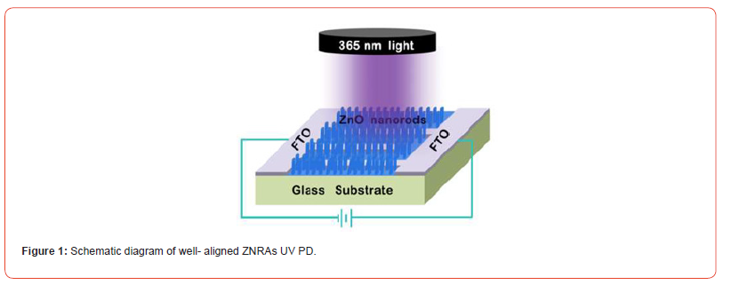
For the preparation of well-aligned ZNRAs UV PD, ZNRAs were placed into a muffle furnace and annealled at 450 °C for 1 h. Figuire 1 presents the schemmatic diagram of this PD (Figure 1).
The morphology of ZNNRAs was examined using a scanning electrron microscopy (SEM, Nova nano SEM 450), their crystal structure wasstudied by an X-ray diffractometer (XRD, Philips X’pert Pro MPD diffractometer). UV-Vis absorption spectrum measurement waas carried out on a spectrophotometer (Shimadzu UV2600). Both transient responses and current-voltage (I-V) characteristics of the PD were recorded by a programmable Keithley 2400, the light sourcewas ahanddheld UV lamp, and a radiometer (UVA3365, Sanpometer) was used to calibrate its optical power density.
Results and Discussionns
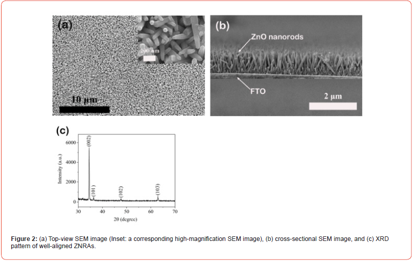
The typical morphologies of the as-grown ZNRAs are presented in Figure 2. In Figure 2(a), we observe that a larrge number of ZnO nanorods densely cover on the substrate. To further discernthe morrphology clearly, in the inset in Figure 2(a), a corresponding high-resolution SEM image is given. The diameters of the nanorods are measured to be 50-70 nm and hexagonal rod-like ZnO can be observed. In Figure 2(b), their cross-sectional SEM image is displayed. Obviously, the nanorods almost grow perpendicular to the substrate, their lengths can be evaluated to be 800-950 nm. XRD pattern of the ZNRAs is exhibited in Figure 2(c). Four diffraction peaks can be distinguished, which correspond to (002) and (101), (102), (103) diffraction peaks of wurtzite (hexagonal) structure of ZnO (JCPDS 36-1451). In particular, we find the primary and sharp (002) diffraction peak, suggesting that the nanorods grow in preferential orientation along the c-axis and have good crystallinity [25,26] (Figure 2).
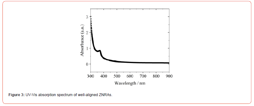
UV-Vis absorption spectrum of ZNRAs was examined, as shown in Figure 3. We note that a absorption edge around 375 nm can be found, a strong absorption in UV region can be clearly observed (Figure 3).
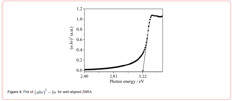
To determine the optical bandgap (Eg) of well-aligned ZNRAs, the optical absorption edge is analyzed by the following Eq. 1[27- 29]:

Where hv, C, and α are photon energy, constant, and absorption coefficient, respectively. From eq. 1, we can obtain the functional dependence of (αhv)2~hv, as plotted in Figure 4. It can be found that the Eg of well-aligned ZNRAs is about 3.22 eV, which approaches bandgap ~3.3 eV of the bulk ZnO (Figure 4).
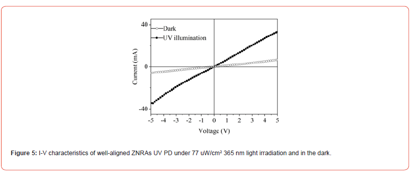
I-V characteristics of ZNRAs PD under UV light irradiation and in the dark are shown in Figure 5. Clearly, when the PD is exposed to UV light, at the same bias, the device currents are much higher than the dark currents, indicating that the UV PDs hows excellent response to 365 nm light. Furthermore, in order to evaluate its performance, several important parameters are obtained [30,31]. The sensitivity (S) can be calculated by the following Eq. 2:

Where Ip and Id are the photocurrent and dark current of ZNRAs UV PD, respectively.
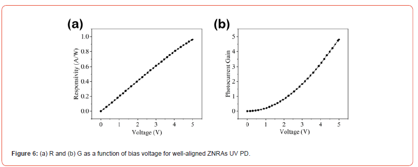
The value of S can be calculated to 37.9 at -0.02 V. Responsivity (R) is another important parameter of the PD, which can be determined using the Eq. 3 [32]:

Where P and A are the incident light intensity (77 μW/cm2) and effective device area (0.36 cm2), respectively. The values of calculated R for ZNRAs UV PD at bias voltages from 0 to 5 V are plotted in Figure 6 (a). The almost linear relationship between the bias voltage and R can be found, the maximum value of R can be estimated to 1.06 A/W at -4.95 V (Figure 5).
Assuming that under ideal conditions, with no external losses, all the photons are absorbed by the UV PD, the photocurrent gain (G) can be given by the following Eq.4 [33]:

Where q is elementary charge, h is Plank’s constant, v is the frequency of absorbed photon. The functional dependence of G versus bias voltage for this ZNRAs UV PD is presented in Figure 6(b). An approximate linear relationship between G and bias voltages can be observed, the maximum G is about 5.22 at -4.95 V.
In addition, the detectivity (D*) for a PD is the reflection of noise. In general, the noise of the PD mainly comes from compound noise, Johnson noise, flicker noise, temperature noise and shot noise, which caused by dark current [34]. If we assume that the noise is entirely caused by the dark current of ZNRAs UV PD, the D* is given by Eq. 5 [35,36]:

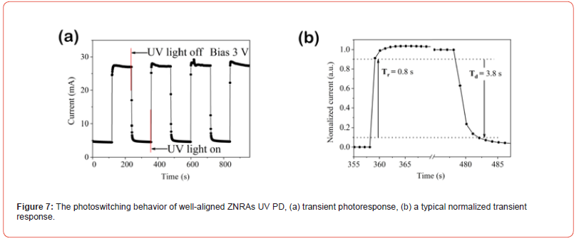
By calculation, the value of D* for this UV PD is 4.60×10⁹ Jones. Figure 7 presents photoswitching behavior of the ZNRAs UV PD. In Figure 7(a), the transient photoresponse characteristics of the PD at 3 V are given, the time-resolved currents contain four light turn on and turn off cycles. Obvious, the device currents can be steadily and quickly switched between the ‘light on’ and ‘light off’ states, it can be verified that the PD show excellent response to 365 nm light, which is entirely consistent with the I-V results. To further determine response speed of the PD, its Tr and Td are estimated, the corresponding normalized transient response curves are plotted, as shown in Figure 7(b). It can be calculated that the Tr and Td are 0.8 s and 3.8 s, respectively. By comparing, the responses of this PD are much faster than those of the UV PDs reported in the previous literatures [34,37,38], which may be attributed to two factors, on the one hand, the well-aligned ZNRAs have good crystallization (as discussed in the XRD analysis), one the other hand, the arrays can provide more direct and effective conduction paths for the photoelectrons [39,40] (Figure 6 & 7).
Conclusions
In summary, well-aligned ZNRAs were successfully fabricated by the facile hydrothermal technique, a UV PD was also built using the resulting ZNRAs as photosensitive layers. The results demonstrated that a fast-response well-aligned ZNRAs UV PD was achieved. This work will provide a valuable reference for the future development of high-performance ZNRAs-based UV PDs.
Acknowledgment
This work was partially supported by the Foundation for Ph.D. Scientific Research of East China University of Technology (No. DHBK2019214), the Open Foundation of Jiangxi Engineering Technology Research Center of Nuclear Geoscience Data Science and System (Grant No. JETRCNGDSS202209), Jiangxi Provincial Graduate Innovation Foundation (No. YC2024-S501), and the Graduate Innovation Foundation of East China University of Technology (No. DHYC-202467).
Conflict of Interest
The authors declare that they have no conflicts of interest.
References
- M Sinha, R Mahapatra, B Mondal, T Maruyama, R Ghosh (2016) J Phys Chem C 120: 3019.
- M Schmitt, S Kuhn, M Wotocek, R Hempelmann (2011) Zeitschrift Fur Phys Chemie 225: 297.
- W Hu, Y Liu, H Yang, X Zhou, C M Li (2011) Biosens Bioelectron 26: 3683.
- A M Hezma, A Rajeh, M A Mannaa (2019) Colloids Surfaces A Physicochem Eng Asp 581: 123821.
- L Li, C Yao, J Gan, K Jiang, Z Hu, et al. (2020) J Phys Chem C 124: 4827.
- E Satheeshkumar, J Yang (2014) RSC Adv 4: 19331.
- T Wang, B Jin, Z Jiao, G Lu, J Ye, et al. (2014) J Mater Chem A 2: 15553.
- D Liu, L Wang, S Ma, Z Jiang, B Yang, et al. (2015) Nanoscale 7: 3627
- S Wang, Y Yang, J Chai, K Zhu, X Jiang, et al. (2016) RSC Adv 6: 64332.
- L N Nguyen, W H Chang, C D Chen, Y W Lan (2014) Nanoscale Horizons 5: 82.
- X Zhang, S Yang, S Bi, A Kumaresan, J Zhou, et al. (2017) RSC Adv 7: 12400.
- Y Jiang, Z Peng, F Wu, Y Xiao, X Jing, et al. (2018) Dalt Trans 47: 8724.
- Y Y Liu, X L Guo, L Zhu, X J Wang, C Ge, et al. (2017) RSC Adv 7: 16924.
- Y H Yang, Y Zhang, N W Wang, C X Wang, B J Li, et al. (2020) Mater Sci Eng C 108, 110490.
- N Lu, H Guo, W Hu, X Wu, X C Zeng (2017) J Mater Chem C 5: 3121.
- Z Cheng, M Yu, G Yang, L Kang (2015) CrystEngComm 17: 1765.
- M Baek, D Kim, K Yong (2017) ACS Appl Mater Interfaces9: 2317.
- D Ghosh, S Kapri, S Bhattacharyya (2016) ACS Appl Mater Interfaces 8: 35496.
- Y Xie, H Li, D Zhang, L Zhang (2019) Vacuum 164: 58.
- Y Zheng, C Chen, Y Zhan, X Lin, Q Zheng, et al. (2007) Inorg Chem 46: 6675.
- L Yin, H Ding, Z Yuan, W Huang, C Shuai, et al. (2018) Opt Mater80: 149.
- P Gu, X Zhu, and D Yang (2020) J Alloys Compd 815: 152346.
- Z Bai, X Yan, X Chen, H Liu, Y Shen, et al. (2013) Curr Appl Phys 13:165.
- O Lupan, G A Emelchenko, V V Ursaki, G Chai, A N Redkin, et al. (2010) Mater Res Bull 45: 1026.
- D K Kwon, Y Porte, K Y Ko, H Kim, J M Myoung (2018) ACS Appl Mater Interfaces 10: 31505.
- Y J Lu, C F Liu, C C Hu, J H Kuo, R Boddula (2017) Mater Chem Phys 189: 56.
- R Gill, S Ghosh, A Sharma, D Kumar, V H Nguyen, et al. (2020) Mater Lett 277: 128295.
- S Park, S Kim, G J Sun, D B Byeon, S K Hyun, et al. (2016) J Alloys Compd 658: 459.
- F H Alsultany, Z Hassan, N M Ahmed (2016) Opt Mater 60: 30.
- Y Su, Z Wu, X Wu, Y Long, H Zhang, et al. (2016) Sensors Actuators, A Phys 241: 169
- Z Yuan, W Wang, H Wu, F Nie, J He (2020) Mater Lett 278: 128413.
- C Li, Y Bando, M Liao, Y Koide, D Golberg, et al. (2010) Appl Phys Lett 161102: 4.
- B D Boruah, D B Ferry, A Mukherjee, A Misra (2015) Nanotechnology 26.
- X Wang, H Wang, W Huang, J Yu (2014) Org Electron 15: 3000.
- R Zou, Z Zhang, J Hu, L Sang, Y Koide, et al. (2013) Nanotechnology 24: 495701.
- A Khayatian, M A Kashi, R Azimirad, S Safa, S F A Akhtarian (2016) Optik 127: 4675.
- Z Yang, M Wang, X Song, G Yan, Y Ding, et al. (2014) J Mater Chem C 2: 4312
- Y Bai, J Zhao, Z Lv, K Lu (2019) Ceram Int 45: 15065.
- F Yi, Q Liao, X Yan, Z Bai, Z Wang, et al. (2014) Phys E Low-Dimensional Syst Nanostructures 61: 180.
-
Zhaolin Yuan*, Weiwei Zeng, Wei Wang, Jianfeng He and Xueyuan Wang. A Fast-Response Ultraviolet Photodetector Based on Hydrothermal Grown Well-Aligned Zno Nanorod Arrays. Insi in Chem & Biochem. 3(2): 2024. ICBC. MS.ID.000557.
-
Biochemical, Nutritional Value, Balanites, Aegyptiaca, Laloub, Seed Oil, Biochemistry, protein, Physicochemical, chloroform, benzene, diethyl.
-

This work is licensed under a Creative Commons Attribution-NonCommercial 4.0 International License.


