 Review Article
Design and Implementation of the Astable Multivibrator
Edward Ong Yong Seng, Nanyang Technological University, VALENS, Singapore.
Received Date: August 01, 2019; Published Date: August 05, 2019
Abstract
This progress report covers the design and implementation of the Astable Multi-vibrator. An Astable Multi-vibrator consists of two amplifying stages connected in a positive feedback loop by two capacitive-resistive coupling networks. The amplifying elements may be junction or field-effect transistors, vacuum tubes, operational amplifiers, or other types of amplifier.
transistors, vacuum tubes, operational amplifiers, or other types of amplifier. The circuit is usually designed in a symmetric form as a cross-coupled pair. Two output terminals can be defined at the active devices, which will have complementary states; one will have high voltage while the other has low voltage, (except during the brief transitions from one state to the other).
Circuitry testing and troubleshooting were carried out in the Astable Multi-vibrator in both designs. The latter wasn’t implemented due to the big difference between the mark/space ratio of 1:100.
Introduction
The circuit has two astable (unstable) states that change alternatively with maximum transition rate because of the “accelerating” positive feedback. It is implemented by the coupling capacitors that instantly transfer voltage changes because the voltage across a capacitor cannot suddenly change. In each state, one transistor is switched on and the other is switched off. Accordingly, one fully charged capacitor discharges (reverse charges) slowly thus converting the time into an exponentially changing voltage. At the same time, the other empty capacitor quickly charges thus restoring its charge (the first capacitor acts as a time-setting capacitor and the second prepares to play this role in the next state). The circuit operation is based on the fact that the forwardbiased base-emitter junction of the switched-on bipolar transistor can provide a path for the capacitor restoration (Figure 1).
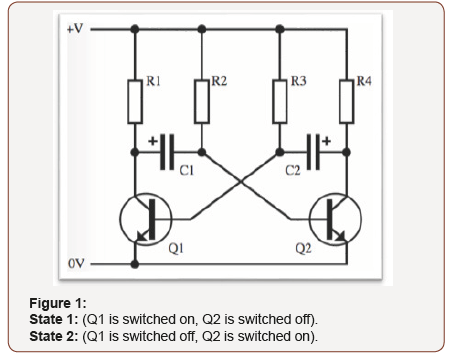
State 1 (Q1 is switched on, Q2 is switched off)
In the beginning, the capacitor C1 is fully charged (in the previous State 2) to the power supply voltage V with the polarity shown in Figure 1. Q1 is on and connects the left-hand positive plate of C1 to ground. As its right-hand negative plate is connected to Q2 base, a maximum negative voltage (-V) is applied to Q2 base that keeps Q2 firmly off. C1 begins discharging (reverse charging) via the high-value base resistor R2, so that the voltage of its righthand plate (and at the base of Q2) is rising from below ground (-V) toward +V. As Q2 base-emitter junction is reverse-biased, it does not conduct, so all the current from R2 goes into C1. Simultaneously, C2 that is fully discharged and even slightly charged to 0.6 V (in the previous State 2) quickly charges via the low-value collector resistor R4 and Q1 forward-biased base-emitter junction (because R4 is less than R2, C2 charges faster than C1). Thus, C2 restores its charge and prepares for the next State C2 when it will act as a time-setting capacitor. Q1 is firmly saturated in the beginning by the “forcing” C2 charging current added to R3 current. In the end, only R3 provides the needed input base current. The resistance R3 is chosen small enough to keep Q1 (not deeply) saturated after C2 is fully charged.
When the voltage of C1 right-hand plate (Q2 base voltage) turns positive and reaches 0.6 V, Q2 base-emitter junction begins diverting a part of R2 charging current. Q2 begins conducting and this starts the avalanche-like positive feedback process as follows. Q2 collector voltage begins falling; this change transfers through the fully charged C2 to Q1 base and Q1 begins cutting off. Its collector voltage begins rising; this change transfers back through the almost empty C1 to Q2 base and makes Q2 conduct more thus sustaining the initial input impact on Q2 base. Thus, the initial input change circulates along the feedback loop and grows in an avalanche-like manner until finally Q1 switches off and Q2 switches on. The forward-biased Q2 base-emitter junction fixes the voltage of C1 right-hand plate at 0.6 V and does not allow it to continue rising toward +V.
State 2 (Q1 is switched off, Q2 is switched on)
Now, the capacitor C2 is fully charged (in the previous State 1) to the power supply voltage V with the polarity shown in Figure 1. Q2 is on and connects the right-hand positive plate of C2 to ground. As its left-hand negative plate is connected to Q1 base, a maximum negative voltage (-V) is applied to Q1 base that keeps Q1 firmly off. C2 begins discharging (reverse charging) via the high-value base resistor R3, so that the voltage of its left-hand plate (and at the base of Q1) is rising from below ground (-V) toward +V. Simultaneously, C1 that is fully discharged and even slightly charged to 0.6 V (in the previous State 1) quickly charges via the low-value collector resistor R2 and Q2 forward-biased base-emitter junction (because R2 is less than R3, C1 charges faster than C2). Thus, C1 restores its charge and prepares for the next State 1 when it will act again as a time-setting capacitor...and so on... (the next explanations are a mirror copy of the second part of State 1).
Multi-Vibrator Frequency
The duration of state 1 (low output) will be related to the time constant R2C1 as it depends on the charging of C1, and the duration of state 2 (high output) will be related to the time constant R3C2 as it depends on the charging of C2. Because they do not need to be the same, an asymmetric duty cycle is easily achieved.
The voltage on a capacitor with non-zero initial charge is:

Looking at C2, just before Q2 turns on, the left terminal of C2 is at the base-emitter voltage of Q1 (VBE_Q1) and the right terminal is at VCC (“VCC” is used here instead of “+V” to ease notation). The voltage across C2 is VCC minus VBE_Q1. The moment after Q2 turns on, the right terminal of C2 is now at 0 V which drives the left terminal of C2 to 0 V minus (VCC - VBE_Q1) or VBE_Q1 - VCC. From this instant in time, the left terminal of C2 must be charged back up to VBE_Q1. How long this take is half our multi-vibrator switching time (the other half comes from C1). In the charging capacitor equation, substituting:
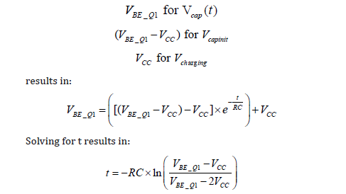
For this circuit to work, VCC>>VBE_Q1 (for example: VCC=5 V, VBE_ Q1=0.6 V), therefore the equation can be simplified to:

The period of each half of the multi-vibrator is therefore given by t = ln (2) RC.
The total period of oscillation is given by:

where...
• f is frequency in hertz.
• R2 and R3 are resistor values in ohms.
• C1 and C2 are capacitor values in farads.
• T is the period (In this case, the sum of two period durations).
For the special case where
• t1 = t2 (50% duty cycle)
• R2 = R3
• C1 = C2

Output Pulse Shape
The output voltage has a shape that approximates a square waveform. It is considered below for the transistor Q1.
During State 1, Q2 base-emitter junction is reverse-biased and capacitor C1 is “unhooked” from ground. The output voltage of the switched-on transistor Q1 changes rapidly from high to low since this low-resistive output is loaded by a high impedance load (the series connected capacitor C1 and the high-resistive base resistor R2).
During State 2, Q2 base-emitter junction is forward-biased and capacitor C1 is “hooked” to ground. The output voltage of the switched-off transistor Q1 changes exponentially from low to high since this relatively high resistive output is loaded by a low impedance load (capacitor C1). This is the output voltage of R2C1integrating circuit.
To approach the needed square waveform, the collector resistors have to be low in resistance. The base resistors have to be low enough to make the transistors saturate in the end of the restoration (RB < β.RC).
Initial Power-Up
When the circuit is first powered up, neither transistor will be switched on. However, this means that at this stage they will both have high base voltages and therefore a tendency to switch on, and inevitable slight asymmetries will mean that one of the transistors is first to switch on. This will quickly put the circuit into one of the above states, and oscillation will ensue. In practice, oscillation always occurs for practical values of R and C.
However, if the circuit is temporarily held with both bases high, for longer than it takes for both capacitors to charge fully, then the circuit will remain in this stable state, with both bases at 0.6 V, both collectors at 0 V, and both capacitors charged backwards to −0.6 V. This can occur at startup without external intervention, if R and C are both very small.
Improvement to the Astable Multi-vibrator
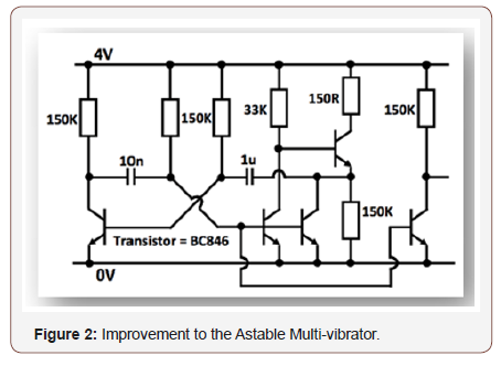
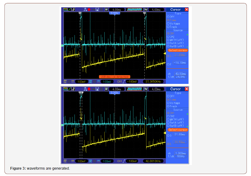
(Figure 2) This design of the Astable Multi-vibrator has been tested but not implemented due to the big difference between the mark and space ratio of 1:100. The waveforms are generated as shown (Figure 3).
Improvement to the Astable Multi-vibrator
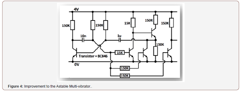
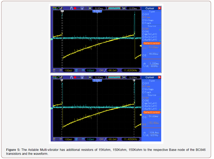
(Figure 4) The Astable Multi-vibrator has additional resistors of 15Kohm, 150Kohm, 150Kohm to the respective Base node of the BC846 transistors and the waveform results are as shown (Figure 5).
Acknowledgement
None.
Conflict of Interest
No conflict of interest.
-
Edward Ong Yong Seng. Design and Implementation of the Astable Multi-vibrator. Glob J Eng Sci. 3(1): 2019. GJES.MS.ID.000554.
-
Accelerating, Astable, Circuit, Voltage, Multi-vibrator frequency, Time period, Frequency, Resistor, capacitor, Pulse shape
-

This work is licensed under a Creative Commons Attribution-NonCommercial 4.0 International License.


