 Review Article
Long Porous Silicon Probe Array for Neural Recordings
Mohamad Hajj-Hassan1* and Houssein Hajj-Hassan2
1Department of Biomedical Engineering, Lebanese International University, Lebanon
2Department of Biological and Chemical Sciences, Lebanese International University, Lebanon
Mohamad Hajj-Hassan, Department of Biomedical Engineering, Lebanese International University, Mazraa, Beirut, P.O.Box 146404, Lebanon.
Received Date: June 10, 2020; Published Date: June 22, 2020
Abstract
Neural probes are the main component of a Brain-Computer Interface (BCI) that enables a communication pathway between the brain and an external device. Neural probes have a wide design space in terms of size, shape, and function. Here, we present novel elongated neural probe with multiple recording sites that can reach than 10mm deep regions in the brain. Reaching such depth offer the possibility of recording of cognitive signals required to operate cognitive prosthetics. The impedance of the recording sites on the probes is on the order of 500 kΩ at 1 kHz, which is suitable for neurophysiological recordings. The probes were made porous using Xenon Difluoride (XeF2) dry etching to improve the biocompatibility and their adherence to the surrounding neural tissue. Numerical studies were performed to determine the reliability of the porous probes. We implanted the elongated probe in rats and show that the elongated probes are capable of simultaneously recording both spikes and local field potentials (LFPs) from various recording sites.
Keywords: Cognitive neural prosthetics; Brain computer interfaces; Porous silicon; Microprobes
Introduction
Brain Computer Interfaces (BCIs) have the potential to improve the lives of paralyzed patients by enabling them to use the electrical activity of their brain to control computers, robots, or even their own limbs [1, 2]. BCIs are intended to function in real time and benefit from real or simulated feedback. The development of BCIs as a direct communication route between the brain and external devices has produced new methods and techniques to connect with and to study the brain [2]. A BCI platform consists of 1) an interface to record neural signals, 2) algorithms to analyze and interpret the recorded neural signals and 3) the external device to be operated and controlled. In this paper, we focus on recording interface composed of a probe implanted in the brain. The probe must be biocompatible, designed to minimize the short term and long-term trauma inflicted during and after insertion. The probes must also be long enough to reach variable depths. Thus, probes must be made durable without increasing their width. Implantable probe arrays have traditionally been metal microprobes [3-5]. However, these have been recently substituted by silicon probes [6-12]. Implanting probes into the brain evokes a tissue response that degrades the recorded signals. Regardless of substrate, probe design must reduce this response to ensure stable and long-term recording.
Relative movement of the probes within the brain causes longterm tissue response due to the difference in mechanical properties between the probes and the neural tissue [13-15]. This process is exacerbated by arrays implanted deep in the brain due to their longer moment arm. Silicon probes can be made thin enough to increase compliance in the brain but without some rigidity, thin probes cannot penetrate neural tissue. Devices to assist implantation have been tested but may still cause neural damage during insertion and can only be used for surface arrays [16,17].
We previously researched methods to develop implantable arrays made from silicon that can record signals from areas that are 6.5mm beneath the brain [18,19]. Considerable progress in the design and fabrication of elongated silicon probes that can reach depths in the brain required for our applications were made. Silicon probes were reinforced probes with metallic structures making them more stable [10].
Tissue Response
The neural injury incurred by probe implantation compromises the integrity of the recorded signals [13, 20,21]. Immune cells isolate the foreign objects by forming as a sheath around the probe [21,22]. This isolates the probes to decrease inflammation and inhibits axon growth. This scaring stabilizes after several weeks [23]. However, recorded signals continue to degrade. The continued presence of the probes leads to persistent inflammation and process that continually damage tissue perpetuating neural loss [24].
Signal degradation can be mitigated by reducing the formation of the glial scar by reducing the immune response, or by the addition of proteins that encourage neural growth around the probe [24-27]. Neural probes impregnated with neural growth factors represent an alternative approach to promote the growth of neurons surrounding the probe [28]. Neurotrophic probes have had much success, particularly in humans, where they have been able to isolate single units for over 4 years [29-31]. Previously, our group has shown nanostructured porous silicon (PSi) surface for implants were showed to improve biocompatibility [32]. Here, we report the use of porous silicon scaffolds, fabricated using Xenon Difluoride (XeF2) dry etching technique, to improve the biocompatibility of the neural probe.
Design and Simulation of the Porous Probe
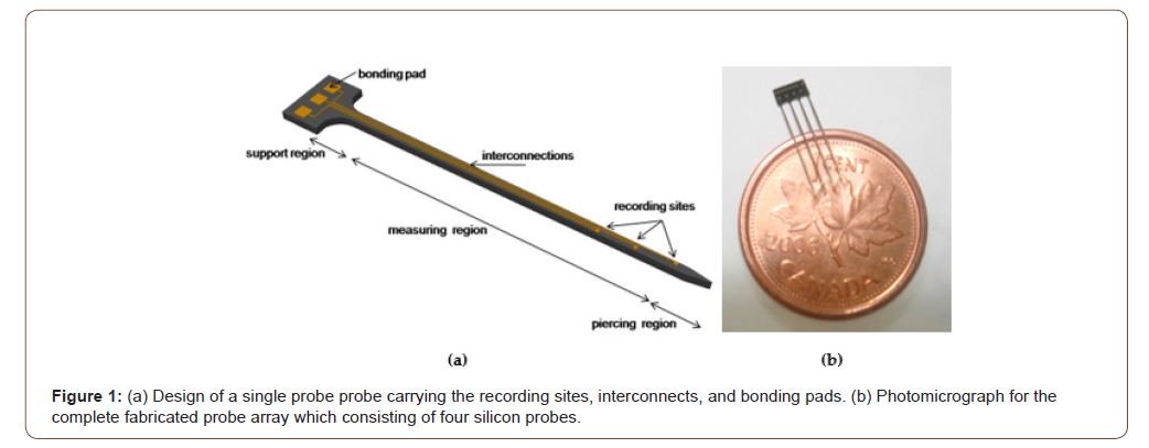
Using microfabrication processes, silicon-based neural probes have well-defined probes holding accurately distributed and spaced recording sites [18]. We manufactured elongated silicon neural probes that can reach 10.5 mm deep into the brain. Figure 1(a) illustrates a single protruding tapered silicon probe that is part of the proposed neural microprobe array consisting of 4 μm probes (as shown in Figure 1(b)) [10, 19]. Each neural probe holds three metallic recording sites to record brain electrical activity, interconnect traces, and back carrier area holding the bonding pads to connect the probes to external read-out electronics. The thickness of the probe array is 50 μm. The length of the probe is 10.5 mm and is divided into a tapered support base region, a measuring region, and a piercing region which are 250 μm, 10 mm, and 250 μm respectively. The tapered base, 350 μm wide, is meant to offer enough strength for each neural probe to withstand surgical implantation. The width of the measuring region gradually reduces along the length of the neural probe in order to minimize brain tissue damage. This region carries several 10 μm x 10 μm gold recording sites to measure neural electrical activities at different depths. To allow an easy entry into the brain, the tip of the neural probe, or piercing region, was shaped into a chisel tip. The distance between the two neighboring probes is 350 μm (Figure 1).
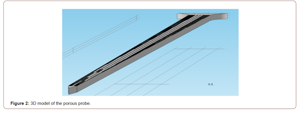
In order to investigate the mechanical strength of the probe, a Finite Element Method (FEM) model of the probe was generated and simulated with the MEMS module in COMSOL Multiphysics. The properties of the silicon used to manufacture the probes were entered into COMSOL. The model structure was meshed into tetrahedral elements with an element size of 4 μm, which was selected so that the simulation converges towards a unique solution. In Figure 2, a layer of porous silicon covers the surface of the probe. The regions of the connecting wires and metal sites are left nonporous. The purpose behind the simulation was to find the failure stresses of the probe due to the forces exerted during and after implantation. The effect of porosity on the mechanical strength of the probe was investigated, due to the fact that the pores represent micro defects that might cause failure. The forces were applied at the tip of the probe since it experiences the most stress during implantation. The imposed forces can be classified into three different cases: (1) under application of two axial forces which are imposed during the penetration phase of the implantation process, (2) under application of a single axial force which occurs directly after penetration and may cause the buckling of the probe, and (3) under application of a vertical force which occurs after the probe implementation and may result in the bending of the probe. In all the 3 cases, the maximum critical stress was yielded by applying increasing stress to the tip of the probe (while fixing its base) until a certain von Mises stress is reached, which is equivalent to the yield stress of a thin silicon cantilever that is approximately equal to 1 GPa [10]. The FEM model of a nonporous probe was used for comparison during all testing cases. For each simulation, a color map of the induced von Mises stress in MPa illustrating the accumulation of the induced stresses on the surface of the probes is plotted (Figure 2).
In case 1, for the non-porous probe a stress of 756 MPa induced the yield stress (1 GPa) at the middle and the tip of the probe as depicted in Figure 3. For the same case, for the porous probe, a stress of 753.7 MPa induced the 1 GPa yield stress in the probe as depicted in Figure 4. In case 2, a stress of 1055 MPa induced the yield stress (1 GPa) at the tip of the probe. As for the porous probe, a stress of 1045 MPa induced the same yield stress. In case 3, a stress of 36.5 MPa induced the yield stress (1 GPa) at the base of the probe as depicted in Figure 5. As for the porous probe, a stress of 23 MPa induced the same yield stress as depicted in Figure 6. First, a direct comparison of the forces that induced the maximum yield stress in the 3 different cases, one can notice the mechanical weakening of the porous silicon probe. The weakening was 0.3 %, 0.1%, 37% in cases 1, 2 and 3 respectively. Nonetheless, this weakening does not significantly risk the mechanical integrity of the neural probe, and this is due to the reason that the force that induced the maximum yield stress of the porous probe is still much higher than the minimum force that the probe must withstand during the penetration of the brain tissue especially for the most significant case 2 (~5MPa [10]). Table 1 summarizes all the simulations conducted for the three cases for porous and non-porous probes. Using the induced stress and the location of application (area of the tip of the probe is 50 μm by 10 μm) the maximum forces endured by the probe can be calculated (Figure 3-6, Table 1).

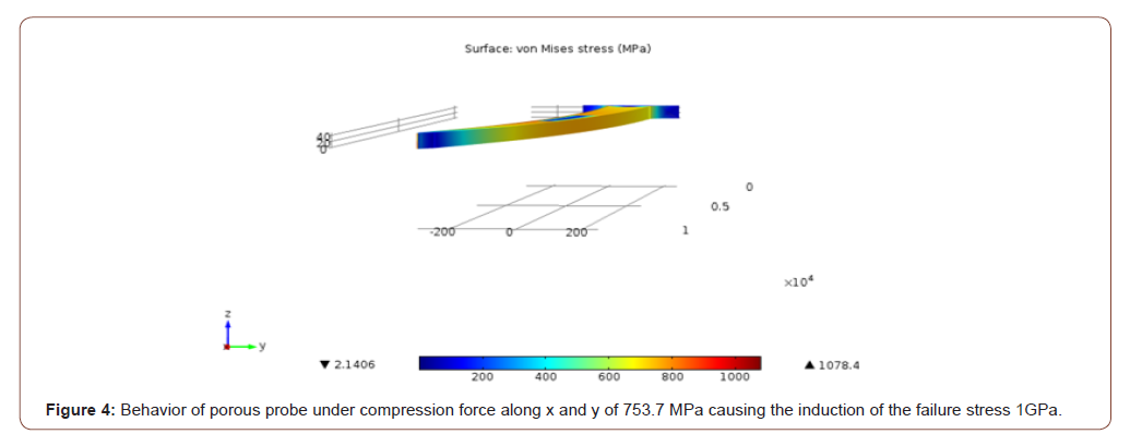
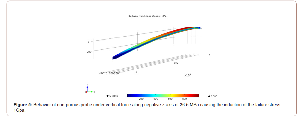
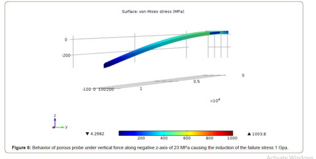
Table 1:Comparison of stresses imposed on porous and non-porous probes in the three different cases (Area of application = 50 μm x 10 μm)

Microfabrication Process
The microfabrication process for the non-porous probe array has been described in detail in our previous publication [19]. In the current work, the microfabrication process follows similar steps at the beginning to form the probe array structure. During the end of the process, we perform additional processing to obtain porous probes. In brief, the microfabrication process begins with dicing a 50 μm thick 4” diameter into small square pieces. A deposition of 500 nm thick adhesion layer of Titanium was followed by deposition a 750 nm thick gold layer. Deposition of both layers was performed using sputtering process. The gold and titanium layers are then patterned using photolithography and wet etched to determine the recording pads, interconnects between the recording sites, and bonding pads. The silicon substrate was then patterned using photolithography and etched using isotropic xenon difluoride (XeF2) dry etching system to define and form the probe structures. The photoresist mask used in the previous step is removed and the silicon probe array is exposed etched using isotropic XeF2 dry etching system to form porous surfaces on the probe array. The formation of porous silicon using XeF2 dry etching system is described in our previous publications [33-35].
A 2μm thick layer of parylene-C, a biocompatible material widely used for coating a broad range of implantable medical devices such as pacemakers [36] and metal-wire neural probes [3], is conformably deposited, at room temperature using a chemical vapor deposition (CVD) system, on the top side of the probe. Parylene-C is needed to insulate the interconnects between the recording sites and bonding pads. Openings to expose the recording sites (used to measure the neural electrical activities) and the bonding pads (for wire-bonding to an external printed circuit board (PCB) for read-out) were defined with photolithography. The exposed parylene-C is etched with oxygen plasma ashing system (PVA TePla Inc., Model: 200).
Figure 7(a) is close-up view of the probe probes clearly showing the chisel-shaped tip, the titanium-gold recording site, and interconnects. Figures 7(b) is a magnified top view of the probe showing the porous silicon area around the recording sites. Figure 7(c) show magnified views of one recording site before and after etching the parylene-C to expose 10 μm x 10 μm gold recording site. Deposition and etching of parylene-C was performed before nanotexturing the probes with XeF2. The bonding pads used to connect the recording sites to external circuitry are shown in Figure 7(d).

The impedance of the recording sites is crucial to the design of neural probes and is mainly controlled by the size of these sites. The measurement of the impedance of the recording sites is conducted by monitoring the electric current while submerging the neural probes in saline solution and circulating current through them. The impedance, at 1 kHz, for the twelve recording sites mounted in the probe was found to be approximately 500 kΩ, a value that meet the requirement of recording both single neuron activity and local field potentials (LFPs) [3].
Testing and Results
The fabricated neural probe was implanted in the barrel cortex of a rat. All implantation procedures were approved by the McGill University Animal Care Committee and were also in compliance with the guidelines of the Canadian Council on Animal Care. A Sprague–Dawley rat underwent handling for few days before the implantation surgery in order to acquaint it with handling by the investigators. The neural probe was tested in the barrel cortex of a rat using a procedure described previously by [3]. Our goal was subcortical nuclei. The probe was centered at 3mm lateral and 2 mm anterior of the bregma and lowered 100-200 micron steps to a depth of 5mm. The dura of the rat was not dissected prior to silicon probe insertion. A thin silver wire was placed under the skin and attached to a screw in the skull for use as an additional ground. The rat was given pain, anti-inflammatory and antibiotic medication as directed by our protocol and the McGill veterinarian. The rat was allowed to recover for at least 1 week before recordings were performed. Spiking activity was recorded using a multi-channel acquisition processor (MAP, Plexon Inc., Dallas, TX, USA) where single units were isolated online using time–voltage windows and their timing and spike waveforms stored on computer. Figure 8(a) shows recordings from six recording sites of the developed neural probe array. Action potential waveforms from multiple neurons are visible in the signal. In particular, several action potential waveforms, or “spikes,” from two neurons, were detected in the neural signal as recorded by the first and the fifth recording sites. Local field potentials (LFPs) were recorded simultaneously from the same recording sites as shown in Figure 8(b).
Conclusions
The purpose of the work reported here is to report the functionality of the developed neural probe in recording neural activity from areas that are 10 mm deep in the brain. A novel methodology to manufacture elongated multi-site neural microprobes with porous silicon surface using XeF2 dry etching was presented. The neural probes with porous surface can help to host neural growth factors to reduce immune response from brain improving biocompatibility and the adherence to the surrounding neural tissue. The probes were inserted through the pia and cortex of living rats to test their penetration ability. Results show a successful insertion of the probe without any bending, shattering, buckling, or breakage. Local field potentials (LFPs) and spiking neural activity were recorded simultaneously from the probe. Long-term implantation studies are required as subsequent work to investigate the effect of the porous silicon surface on the performance and function of the probe.
Acknowledgement
None.
Conflict of Interest
No conflict of interest.
References
- Andersen RA, EJ Hwang, GH Mulliken (2010) Cognitive Neural Prosthetics. Annual Review of Psychology 61: 169-190.
- Hatsopoulos NG, JP Donoghue (2009) The science of neural interface systems. Annu Rev Neurosci 32: 249-266.
- Musallam S, Martin B, Philip T, Richard A (2007) A floating metal microelectrode array for chronic implantation. J Neurosci Methods 160(1): 122-127.
- Williams JC, RL Rennaker, DR Kipke (1999) Stability of chronic multichannel neural recordings: Implications for a long-term neural interface. Neurocomputing 26-27: p. 1069-1076.
- Kralik JD, D F Dimitrov, D J Krupa, D B Katz, D Cohen, et al. (2001) Techniques for long-term multisite neuronal ensemble recordings in behaving animals. Methods 25(2): 121-150.
- Drake KL, KD Wise, J Farraye, DJ Anderson, SL BeMent (1988) Performance of Planar Multisite Microprobes in Recording Extracellular Single-Unit Intracortical Activity. Ieee Transactions on Biomedical Engineering 35(9): 719-732.
- Hetke JF, DJ Anderson, KD Wise (1997) Design ranges for silicon multichannel neural probes. Proceedings of the 18th Annual International Conference of the Ieee Engineering in Medicine and Biology Society 18: 266-267.
- Campbell PK, KE Jones, RJ Huber, KW Horch, RA Normann (1991) A silicon-based, three-dimensional neural interface: manufacturing processes for an intracortical electrode array. IEEE Trans Biomed Eng 38(8): 758-68.
- Kipke DR, Rio J Vetter, Justin C Williams, Jamille F Hetke (2003) Silicon-substrate intracortical microelectrode arrays for long-term recording of neuronal spike activity in cerebral cortex. IEEE Trans Neural Syst Rehabil Eng 11(2): 151-155.
- Hajj-Hassan M, V Chodavarapu, S Musallam (2009) Reinforced silicon neural microelectrode array fabricated using a commercial MEMS process. Journal of Micro-Nanolithography Mems and Moems 8(3): 033011.
- Z Fekete, E Pálfi, G Márton, M Handbauer, Zs Bérces, et al. (2015) In Vivo Iontophoretic BDA Injection through a Buried Microfluidic Channel of a Neural Multielectrode, Procedia Engineering 120: 464-467.
- F Michon, Arno Aarts, Tobias Holzhammer, Patrick Ruther, Gustaaf Borghs, et al. (2016) Integration of silicon-based neural probes and micro-drive arrays for chronic recording of large populations of neurons in behaving animals 13(4).
- He W, GC McConnell TM, Schneider RV, Bellamkonda, et al. (2007) A novel anti-inflammatory surface for neural electrodes. Advanced Materials 19(21): 3529-3533.
- Lee H, Ravi V Bellamkonda, Wei Sun, Marc E Levenston (2005) Biomechanical analysis of silicon microelectrode-induced strain in the brain. Journal of Neural Engineering 2(4): 81-89.
- Subbaroyan J, DC Martin, DR Kipke (2005) A finite-element model of the mechanical effects of implantable microelectrodes in the cerebral cortex. Journal of Neural Engineering 2(4): 103-113.
- Brien DPO, TR Nichols, MG Allen (2001) Flexible microelectrode arrays with integrated insertion devices. in Micro Electro Mechanical Systems, 2001. MEMS 2001. The 14th IEEE International Conference on. 2001.
- Rousche PJ, RA Normann (1992) A method for pneumatically inserting an array of penetrating electrodes into cortical tissue. Ann Biomed Eng 20(4): 413-422.
- Hajj Hassan M, V Chodavarapu, S Musallam (2008) NeuroMEMS: Neural Probe Microtechnologies. Sensors 8(10): 6704-6726.
- Hajj-Hassan M, VP Chodavarapu, S Musallam (2009) Microfabrication of ultra-long reinforced silicon neural electrodes. Micro & Nano Letters 4(1): 53-58.
- Bridges AW, Rachel E Whitmire, Neetu Singh, Kellie L Templeman, Julia E Babensee, et al. (2010) Chronic inflammatory responses to microgel-based implant coatings. J Biomed Mater Res A 94(1): 252-258.
- Szarowski DH, M D Andersen, S Retterer, A J Spence, M Isaacson, et al. (2003) Brain responses to micro-machined silicon devices. Brain Res 983(1-2): 23-35.
- Turner JN, W Shain, DH Szarowski, M Andersen, S Martins, et al. (1999) Cerebral astrocyte response to micromachined silicon implants. Exp Neurol 156(1): 33-49.
- Ludwig KA, Jeffrey D Uram, Junyan Yang, David C Martin, Daryl R Kipke, et al. (2006) Chronic neural recordings using silicon microelectrode arrays electrochemically deposited with a poly(3,4-ethylenedioxythiophene) (PEDOT) film. Journal of Neural Engineering 3(1): 59-70.
- McConnell GC, Howard D Rees, Allan I Levey, Claire-Anne Gutekunst, Robert E Gross, et al. (2009) Implanted neural electrodes cause chronic, local inflammation that is correlated with local neurodegeneration. J Neural Eng 6(5): 056003.
- Kozai TD, Nicholas B. Langhals, Paras R. Patel, Xiaopei Deng, Huanan Zhang, et al. (2012) Ultrasmall implantable composite microelectrodes with bioactive surfaces for chronic neural interfaces. Nat Mater 11(12): 1065-1073.
- Kim DH, M Abidian, DC Martin (2004) Conducting polymers grown in hydrogel scaffolds coated on neural prosthetic devices. J Biomed Mater Res A 71(4): 577-585.
- Kim DH (2008) Soft, Fuzzy, and Bioactive Conducting Polymers for Improving the Chronic Performance of Neural Prosthetic Devices, in Indwelling Neural Implants: Strategies for Contending with the In Vivo Environment, W.M. Reichert, Editor.: Boca Raton (FL).
- Wadhwa R, CF Lagenaur, XT Cui (2006) Electrochemically controlled release of dexamethasone from conducting polymer polypyrrole coated electrode. J Control Release 110(3): 531-541.
- Howell B, WM Grill (2015) 4 - Design of electrodes for stimulation and recording A2 - Kilgore, Kevin, in Implantable Neuroprostheses for Restoring Function. Woodhead Publishing: 59-93.
- Bartels J, Dinal Andreasen, Princewill Ehirim, Hui Mao, Steven Seibert, et al. (2008) Neurotrophic electrode: Method of assembly and implantation into human motor speech cortex. Journal of Neuroscience Methods 174(2): 168-176.
- Thompson CH, Marissa J Zoratti, Nicholas B Langhals, Erin K Purcell (2016) Regenerative Electrode Interfaces for Neural Prostheses. Tissue Engineering Part B-Reviews 22(2): 125-135.
- Mohamad Hajj-Hassan, Maedeh Khayyat-Kholghi, Huifen Wang, Vamsy Chodavarapu, Janet E Henderson (2011) Response of murine bone marrow-derived mesenchymal stromal cells to dry-etched porous silicon scaffolds. Journal of Biomedical Materials Research Part A 99a(2): 269-274.
- Hajj-Hassan M, M Cheung, V Chodavarapu (2010) Dry etch fabrication of porous silicon using xenon difluoride. Micro & Nano Letters 5(2): 63-69.
- Hajj-Hassan M, MC Cheung, VP Chodavarapu (2011) Ultra-thin porous silicon membranes fabricated using dry etching. Micro & Nano Letters 6(4): 226-228.
- Cheung MCK, Philip JR Roche, Mohamad Hajj-Hassan, Andrew K Kirk, Zetian Mi, et al. (2011) Controlling optical properties and surface morphology of dry etched porous silicon (vol 5, 053503, 2011). Journal of Nanophotonics 5.
- Hsu JM, Loren Rieth, Richard A Normann, Prashant Tathireddy, Florian Solzbacher (2009) Encapsulation of an Integrated Neural Interface Device With Parylene C. Ieee Transactions on Biomedical Engineering 56(1): 23-29.
-
Mohamad Hajj-Hassan, Houssein Hajj-Hassan. Long Porous Silicon Probe Array for Neural Recordings. Arch Neurol & Neurosci. 8(1): 2020. ANN.MS.ID.000678.
-
Cognitive neural prosthetics; Brain computer interfaces; Porous silicon; Microprobes.
-

This work is licensed under a Creative Commons Attribution-NonCommercial 4.0 International License.


